System with Recessed Sensing or Processing Elements

Active Publication Date: 2011-03-10
ANALOG DEVICES INC
View PDF74 Cites 66 Cited by
  • Summary
  • Abstract
  • Description
  • Claims
  • Application Information

AI Technical Summary

Benefits of technology

[0007]In a first embodiment of the invention there is provided a substrate having a frontside surface comprising circuitry, and a backside surface comprising a plurality of recesses. A plurality of the recesses have at least one sensor, and a port configured to expose the sensor to the environment external to the recess. A sensor may detect a characteristic of the external environment, or energy from the environment that impinges on the sensor. Some embodiments employ inertial sensors without exposing the inertial sensors directly to the external environment. The frontside of the substrate may include circuitry configured to receive a sig

Problems solved by technology

The chip 200 is exposed to its environment without the benefit of a surrounding package, and is therefore susceptible to damage from contact with other objects in the environment, in addition to other environmental factors, such as heat, dust, humidity, etc.
Another consequence of this approach is that one sensor may be some distance from another sensor, possibly hampering their ability to sense or measure the same local environment.
Spreading out the components 301 also requires longer interconnection conductors than a more compact layout, possibly leading to increased parasitic capacitances, or increased susceptibility to noise coupling to the signals.

Method used


Image

  • System with Recessed Sensing or Processing Elements
  • System with Recessed Sensing or Processing Elements
  • System with Recessed Sensing or Processing Elements

Examples


embodiment 1200

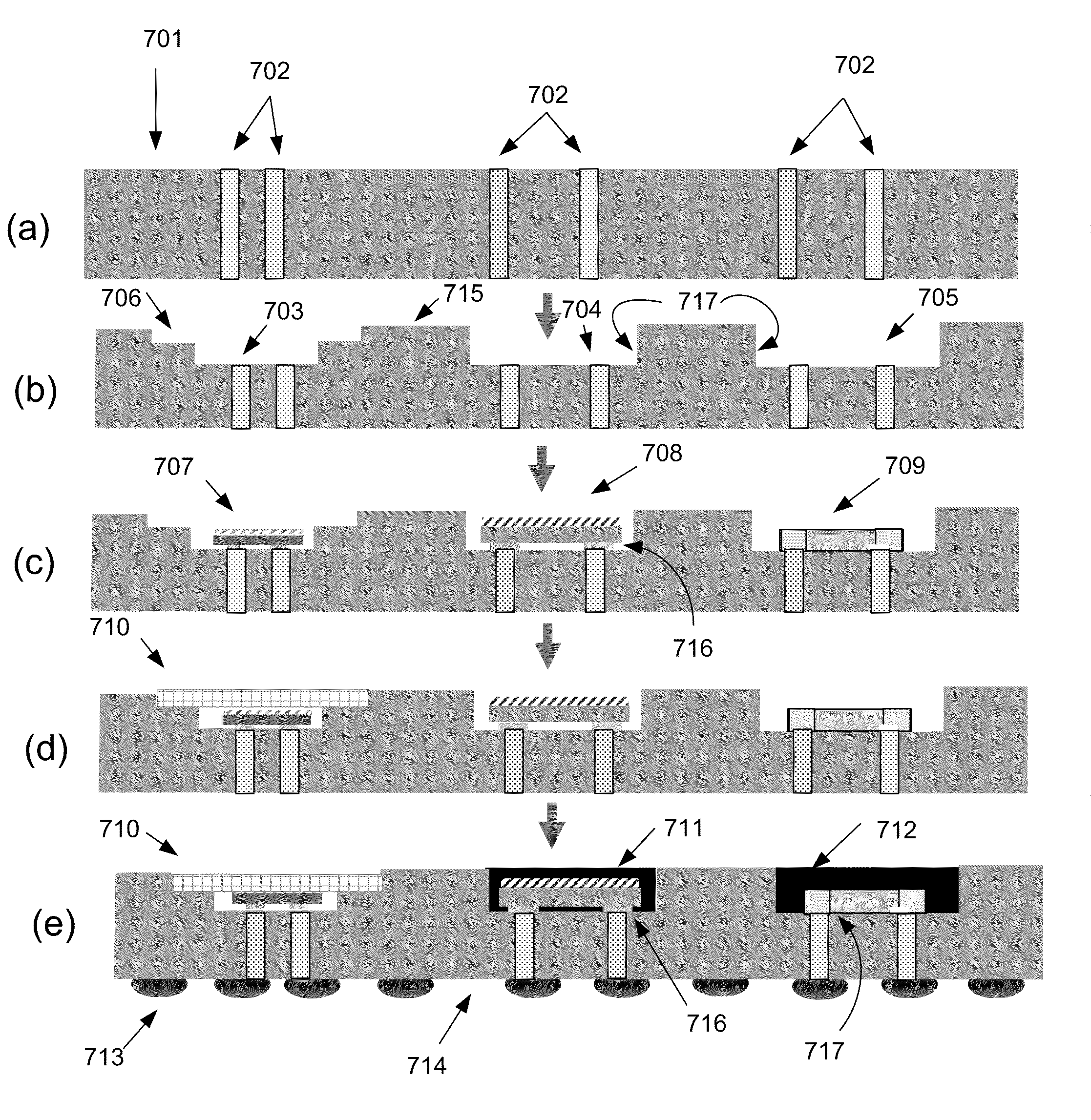
[0074]One such embodiment 1200 is schematically illustrated in FIG. 12. The laminate base 1201 includes multiple layers [such as 1201(a) and 1201(b)], which may alternate in material or electrical conductivity. For example, some embodiments may include layers that are insulators, layers that are power or ground planes, and layers that include conductors to transmit signals from one point in the base to another.

[0075]A recess 1202 in a laminate base 1201 may be created by an aperture 1203 in a layer 1201(a) of the laminate base 1201, or a plurality of aligned apertures in two or more of the layers 1201(a), 1201(b) and 1201(c). A recess may be open to the environment, or may be closed-off from the environment. A cap 1204 above a recess 1205 may be formed by a layer 1201(b) above the recess. In some embodiments, a sensor or integrated circuit 1204 may occupy a layer above the recess 1205, and partially or completely close-off the recess 1205 from the external environment. A cap, lens, ...

embodiment 1300

[0076]FIG. 13 schematically illustrates an embodiment 1300 of a laminated base 1301, and specifically illustrates details of the laminate near an edge 1302 of the laminated base. To resist de-lamination, such as from thermal stress, various layers 1303, 1304, 1305 may be made to interlock. For example, interlocking may be facilitated by increasing the surface area between two adjoining layers 1303, 1304 by having one layer 1304 extend into the other 1303, while causing the other layer 1303 to cover the extension. In an alternate embodiment, layer 1306 extends into layer 1307 by extending fingers or vias 1308 between layers. In a preferred embodiment, such interlocking features are in the region of singulation to mitigate propagation of cracks or delamination from the edges.

[0077]A cover, cap, filter, or lens in a laminate base may be at or near a surface of the laminate base, as highlighted in FIG. 14A. The cover, cap, filter, or lens 1401 may include openings serrated edges 1402 to...

embodiment 1700

[0082]In this embodiment 1700, the laminate substrate 1701 (containing the sensing structures, lenses, filters, etc., 1707, 1708) is mounted on a silicon substrate or integrated circuit 1702, which may include circuitry to drive or control the sensing system 1700 or its individual sensors 1707, 1708, or process the output of one or more of the sensors 1707, 1708. An advantage of such an embodiment is that the laminate substrate 1701, or other such embedded structure, could be tailored to suit different sensing applications as required, simply by designing variations that all mount to the same processing integrated circuit. The processing integrated circuit 1702 could be, for example, a digital signal processor (“DSP”), an application-specific integrated circuit (“ASIC”) or other integrated circuit adapted to mount to and electrically communicate with the laminate substrate 1701.

[0083]A variety of laminate substrates 1701 may be adapted to mount to one design of integrated circuit 17...


PUM


Abstract

Backside recesses in a base member host components, such as sensors or circuits, to allow closer proximity and efficient use of the surface space and internal volume of the base member. Recesses may include covers, caps, filters and lenses, and may be in communication with circuits on the frontside of the base member, or with circuits on an active backside cap. An array of recessed components may a form complete, compact sensor system.

Description

TECHNICAL FIELD [0001]The present invention relates to electronic assemblies, and more particularly to electronic assemblies with embedded sensors and processing circuitry.BACKGROUND ART [0002]Electronic assemblies may be composed of a number of components. It is known in the art to mount sensor and signal processing components to a surface of a substrate. Some applications, known as “flip chip,” mount integrated circuits directly to a surface of a substrate. Other applications house a sensor or integrated circuit in a package. The package may include a lead frame, with one or more die are mounted on the leadframe. The leadframe and die are then encapsulated, and the package is mounted to a substrate, such as a printed circuit board, for example. It is known to increase the density of components on a substrate by stacking several integrated circuits within a single package, such as in U.S. Pat. No. 6,784,023, entitled “Method Of Fabrication Of Stacked Semiconductor Devices,” or U.S....

Claims


Application Information

Patent Timeline
IPC IPC(8): H01L29/84H01L21/52
CPCB81C1/0023B81B3/0018H01L2224/16225H01L2924/15156H01L2924/15311H01L2924/1461H01L2924/19105H01L2224/16145H01L2924/00H01L2224/16235H01L2224/94H01L2224/13025H01L2924/14H01L2224/14181H01L2224/16146H01L2224/81
Inventor O'DONNELL, ALAN J.CUSACK, MICHAEL J.MCGEEHAN, RIGAN F.GRIFFIN, GARRETT A.
Owner ANALOG DEVICES INC
Why Eureka
Try Eureka