
Semiconductor integrated circuit

a technology of integrated circuits and semiconductors, applied in the direction of instruments, generating/distributing signals, pulse techniques, etc., can solve the problems of insufficient reduction of clock skew, clock skew occurring between, clock skew, etc., to reduce power consumption, reduce clock skew, and reduce clock skew

Inactive Publication Date: 2011-03-10
RENESAS ELECTRONICS CORP
View PDF10 Cites 4 Cited by
  • Summary
  • Abstract
  • Description
  • Claims
  • Application Information

AI Technical Summary

Benefits of technology

[0008]A semiconductor integrated circuit 100 shown in FIG. 5 includes an Always-ON area 102 and a power supply separation area 103. When the semiconductor integrated circuit 100 operates, the Always-ON area 102 is always supplied with the power supply. Even when the semiconductor integrated circuit 100 operates, the power supply separation area103 in which the power supply is supplied or shut off independently of the Always-ON area 102. For example, the semiconductor integrated circuit 100 is mounted in a mobile phone, and the power supply separation area 103 in which a circuit that carries out a processing of a camera function is laid out. This enables to reduce the power consumption by shutting off the power supply supplied to the power supply separation area 103, when the camera function is not started and thus it is necessary to drive the circuit that carries out the processing of the camera function.
[0027]In accordance with each of the above-described exemplary aspects, in a semiconductor integrated circuit includes areas in which the power supply is independently supplied or shut off, the present invention provide a semiconductor integrated circuit that is capable of reducing the clock skew and reducing the power consumption.

Problems solved by technology

In a semiconductor integrated circuit, there is a major problem to reduce the clock skew occurred by difference of wiring length from a source of a clock signal to circuits which receive the clock signal, wiring resistance and so on.
Thus, there is a problem that the clock skew is occurred between the area 102 and the area 103.
Consequently, a technique disclosed in Japanese Unexamined Patent Application Publication No. 2007-214334 cannot enough reduce the clock skew.
As a result, the power supply separation area 203 is supplied with the normally unnecessary clock signal, thus there is a problem that the extra power supply is consumed.
That is, there is a problem that the semiconductor integrated circuit 200 shown in FIG. 6 can reduce the clock skew between the area 202 and the area 203, but cannot enough reduce the power consumption.
The abovementioned problem is occurred not only a semiconductor integrated circuit that includes areas in which the power supply is independently supplied or shut off.
That is, as described above, there is a similar problem not only a semiconductor integrated circuit that the areas in each of which the clock signal and the power supply are independently supplied or shut off but also a semiconductor integrated circuit that the areas in each of which the clock signal is independently supplied or shut off.
Thus, there is problem that the clock skew is occurred between each of the areas.
That is, there is a problem that the power consumption can be reduced but the clock skew is occurred between each of the areas as with the semiconductor integrated circuit 100 shown FIG. 5.
As a result, the power supply separation area 203 is supplied the normally unnecessary clock signal, thus there is a problem that the extra power is consumed.
As explained above, in a semiconductor integrated circuit includes areas in which the power supply is independently supplied or shut off, there is a problem to do not reduce the clock skew and do not reduce the power consumption.

Method used


Image

  • Semiconductor integrated circuit
  • Semiconductor integrated circuit
  • Semiconductor integrated circuit

Examples


first exemplary embodiment

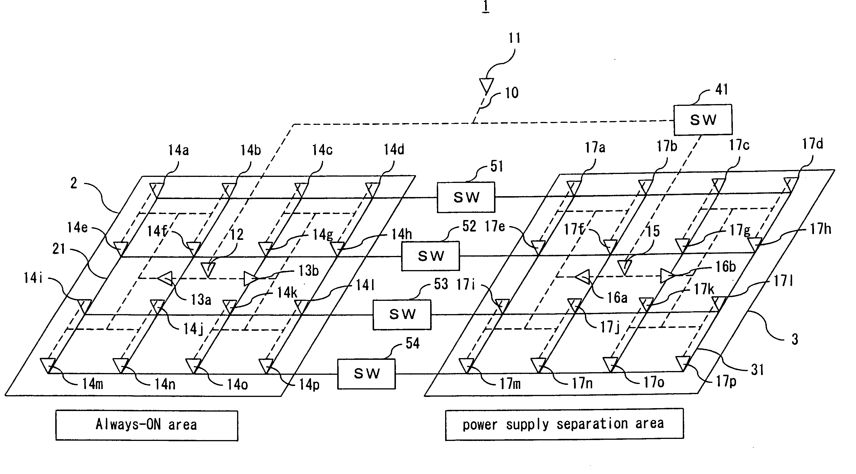
[0035]A configuration of a semiconductor integrated circuit in accordance with a first exemplary embodiment of the present invention is explained with reference to FIG. 1. FIG. 1 is a configuration diagram of a semiconductor integrated circuit in accordance with a first exemplary embodiment of the present invention.

[0036]A semiconductor integrated circuit 1 includes a Always-ON area 2, a power supply separation area 3, a clock tree 10, a clock root buffer 11, a switch (hereafter, referred to as a “clock tree”) 41 and switches 51, 52, 53, and 54. The clock tree 10 includes the clock root buffer 11.

[0037]The clock tree 10 branches in the subsequent stage of the clock root buffer 11. The clock tree 10, in a tree shape wire (hereafter, referred to as a “branch”) in the Always-ON area 2, includes a clock buffer 12 in the next stage of the clock root buffer 11, clock buffers 13a and 13b in the next stage of the clock buffer 12, and clock buffers 14a-14p in the next stage of the clock buff...

second exemplary embodiment

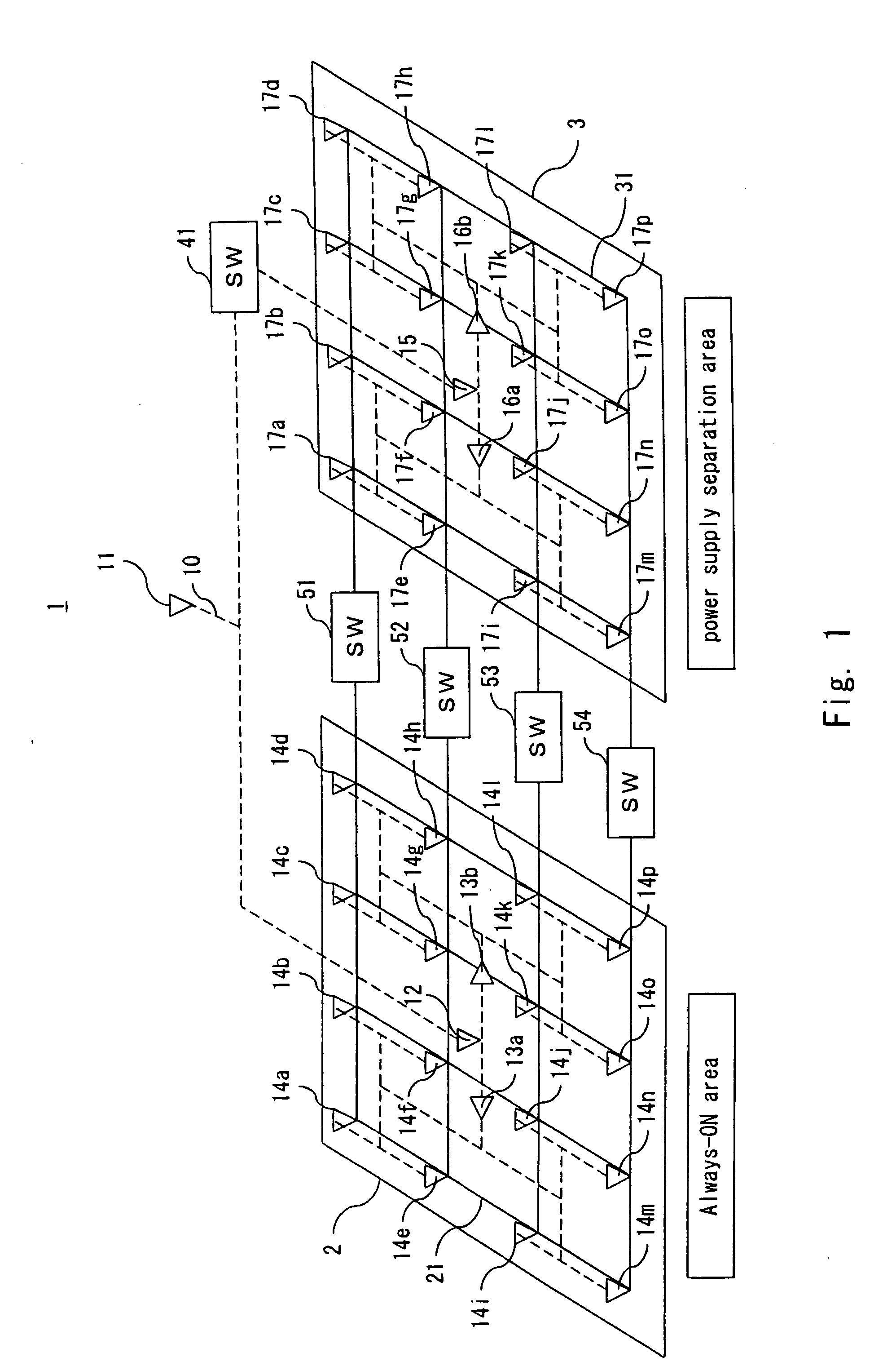
[0057]A configuration of a semiconductor integrated circuit in accordance with a second exemplary embodiment of the present invention is explained with reference to FIG. 2. FIG. 2 is a configuration diagram of a semiconductor integrated circuit in accordance with a second exemplary embodiment of the present invention.

[0058]The semiconductor integrated circuit 1 in accordance with a second exemplary embodiment of the present invention is a semiconductor integrated circuit 1 is, in accordance with a first exemplary embodiment of the present invention, in which the Always-ON area 2 includes a drive target circuit 25 and the power supply separation area 3 includes a drive target circuit 35.

[0059]In the second exemplary embodiment of the present invention, as shown in FIG. 2, the SWs 51-53 are laid out at a position that corresponds to the place laid out the drive target circuits 22 and 32 of the clock mesh 21 and the clock mesh 31.

[0060]As explained in the related arts, the reason why t...

third exemplary embodiment

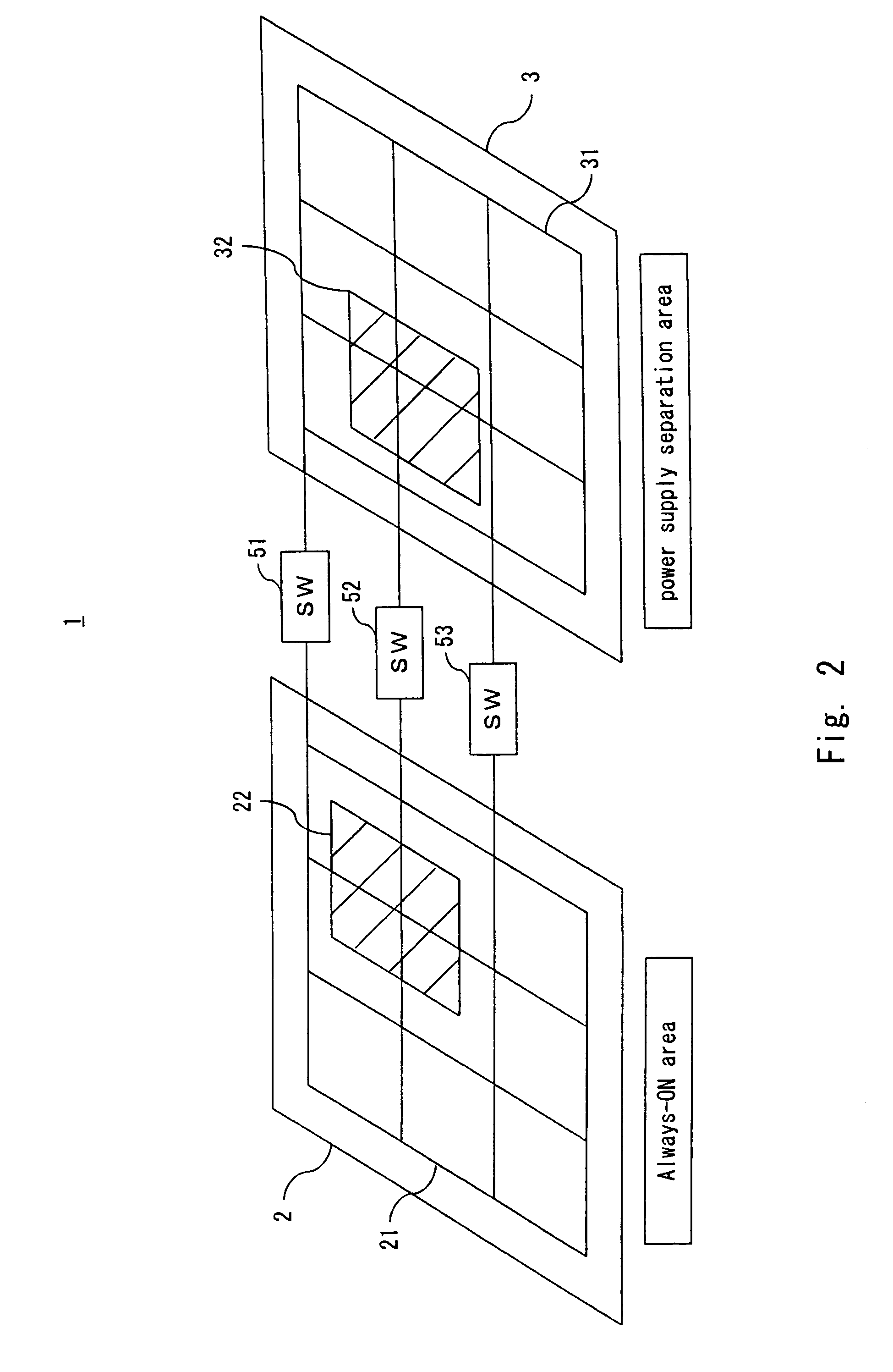
[0064]A configuration of a semiconductor integrated circuit in accordance with a third exemplary embodiment of the present invention is explained with reference to FIG. 3. FIG. 3 is a configuration diagram of a semiconductor integrated circuit in accordance with a third exemplary embodiment of the present invention.

[0065]The semiconductor integrated circuit 1 in accordance with a third exemplary embodiment of the present invention includes the Always-ON area 2 and the power supply separation area 3 as with the first exemplary embodiment of the present invention. The Always-ON area 2 includes clock meshes 23 and 24, and a drive target circuits 25 and 26. The power supply separation area 3 includes clock meshes 33 and 34, and the drive target circuits 35 and 36.

[0066]The clock meshes 23, 24, 33, and 34 are supplied with a clock signal from the clock tree (not shown) to reduce the clock skew each of the Always-ON area 2 and the power supply separation area 3.

[0067]The clock mesh 23 sup...


PUM


Abstract

A semiconductor integrated circuit 1 according to an exemplary embodiment of the present invention is including: a first wire that is supplied with a clock signal; a second wire that is supplied with the clock signal, the clock signal is supplied or shut off independently of the clock signal supplied to the first wire; a first area that includes a first mesh shape wire supplied with the clock signal from the first wire; a second area that includes a second mesh shape wire supplied with the clock signal from the second wire; and a switching circuit that switches to a conduction or a shutoff of a signal transmitted between the first mesh shape wire and the second mesh shape wire.

Description

INCORPORATION BY REFERENCE[0001]This application is based upon and claims the benefit of priority from Japanese patent application No. 2009-205580, filed on Sep. 7, 2009, the disclosure of which is incorporated herein in its entirety by reference.BACKGROUND[0002]1. Field of the Invention[0003]The present invention relates to a semiconductor integrated circuit, and more particularly, a technique to reduce the clock skew and the power consumption of the semiconductor integrated circuit.[0004]2. Description of Related Art[0005]In a semiconductor integrated circuit, there is a major problem to reduce the clock skew occurred by difference of wiring length from a source of a clock signal to circuits which receive the clock signal, wiring resistance and so on. If the clock skew is occurred, a semiconductor integrated circuit malfunctions by that the deviation in operation timing of each of circuits supplied with a clock signal is occurred.[0006]Japanese Unexamined Patent Application Public...

Claims


Application Information

Patent Timeline
Patent Type & Authority Applications(United States)
IPC IPC(8): H03K17/00
CPCY02B60/1278Y02B60/1282G06F1/10H03K19/0016G06F1/3203G06F1/3287Y02D10/00
Inventor TERAYAMA, TOSHIAKI
Owner RENESAS ELECTRONICS CORP
Features
  • Generate Ideas
  • Intellectual Property
  • Life Sciences
  • Materials
  • Tech Scout
  • Unparalleled Data Quality
  • Higher Quality Content
  • 60% Fewer Hallucinations
Learn More