Optimization method of multi-level gating clock network in nanotechnology

A gated clock and clock network technology, applied in the electronic field, can solve problems such as single structure and limited effect of multi-level gated clock design, and achieve the effects of reducing clock deviation, regular clock structure, and increasing clock common paths

Active Publication Date: 2018-02-16
NAT UNIV OF DEFENSE TECH
View PDF4 Cites 0 Cited by
  • Summary
  • Abstract
  • Description
  • Claims
  • Application Information

AI Technical Summary

Problems solved by technology

However, the mesh clock structure is also only suitable for relatively simple clock structures with no gating clock or only one level of gating clock
[0011] The above methods all increase the proportion of the common path of the clock to varying degrees, but they are only applicable to a clock structure with a single structure, and the design effect for multi-level gated clocks is limited.
However, with the development of the microelectronics industry, the design of multi-level gated clocks is becoming more and more common, and how to reduce the clock skew and its uncertainty of such designs has become more and more difficult

Method used


Image

  • Optimization method of multi-level gating clock network in nanotechnology
  • Optimization method of multi-level gating clock network in nanotechnology
  • Optimization method of multi-level gating clock network in nanotechnology

Examples


Embodiment Construction

[0036] The present invention will be described in further detail below in conjunction with the accompanying drawings and embodiments.

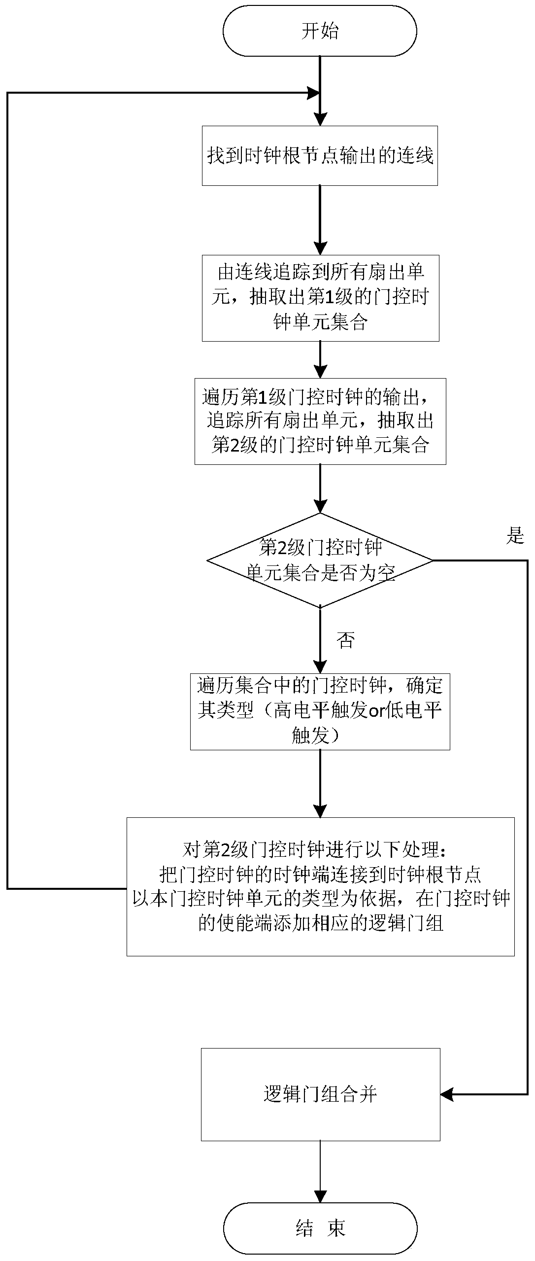
[0037] Such as figure 1 As shown in the figure, it is a flow chart of reducing the multi-level gating clock to level 1. The specific process is as follows:

[0038] (11) Starting from the clock root node, find its connection;

[0039] (12) From all the units traced to the fan-out by the connection, find out all the gated clock units directly connected to the clock root node to form a set of the first-level gated clock units;

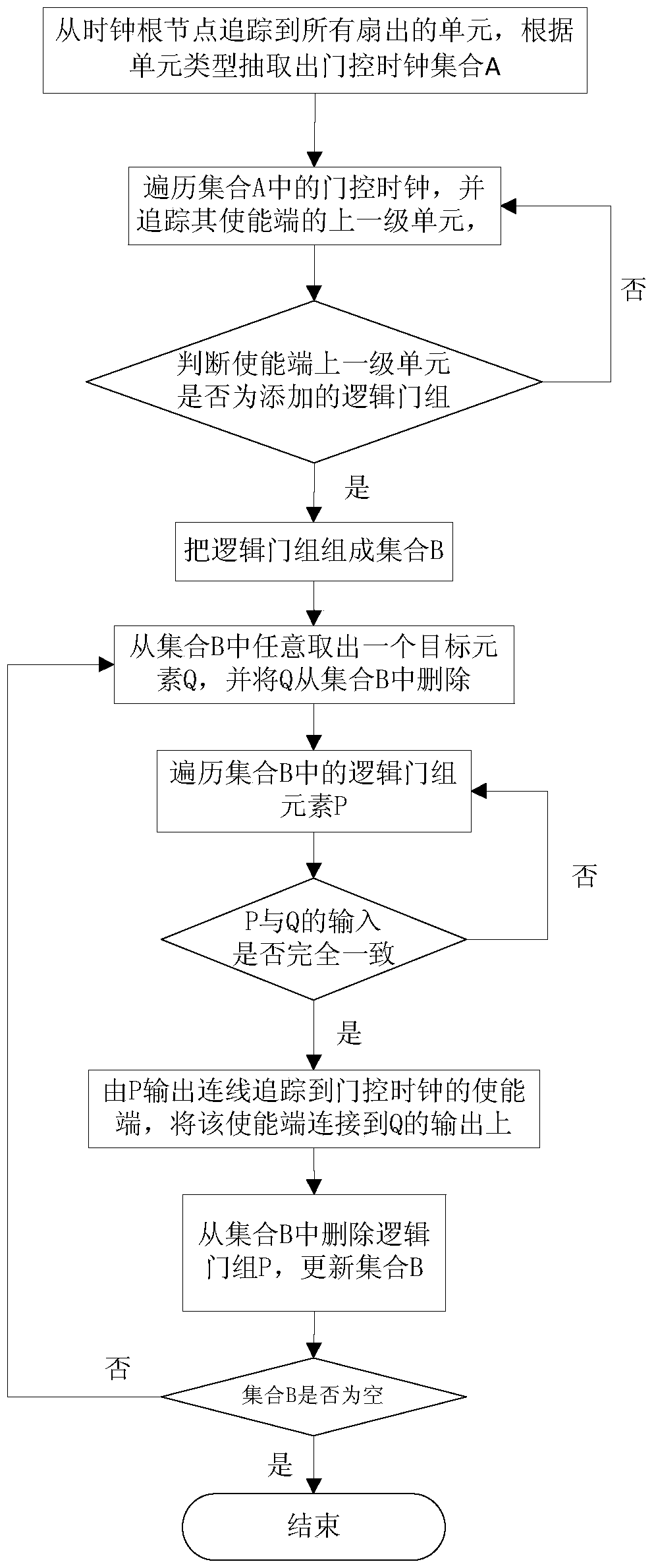
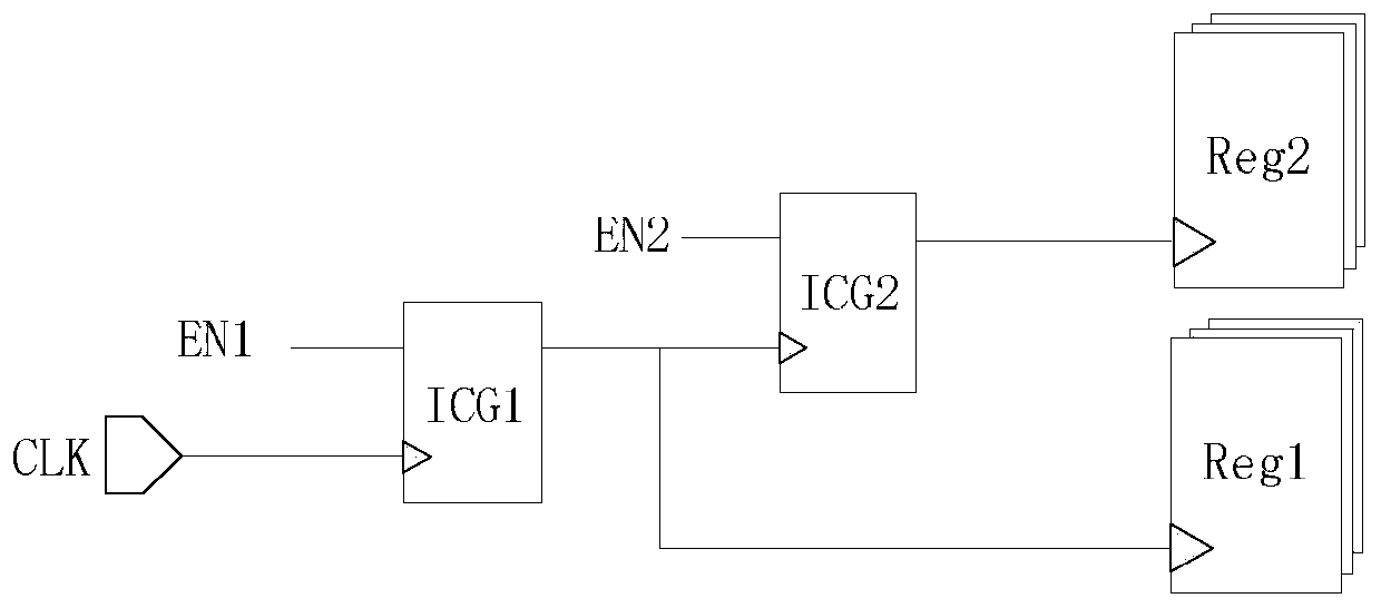
[0040] (13) Traverse each element (i.e., the gated clock unit) in the set of the first-level gated clock unit obtained in step (12) to perform the following operations: ① detect the type of the gated clock unit (high level trigger or low-level trigger) and record, ②find and record the connection of the enable terminal input of the gated clock unit, and record, ③find and record the connection of the output terminal of t...


PUM


Abstract

The invention belongs to the technical field of electrons and relates to a multistage gated clock network optimization method in a nanometer technology; the method comprises the steps of assuming that a network has N stages of gated clocks, Kn gated clock units exist in the nth stage, degrading nth-grade gated clocks, wherein n is larger than 1, and the degrading steps are as follows: (1) finding out all 2nd-stage gated clocks in a circuit, a total of K2; (2) for K2 gated clock units in the 2nd stage, disconnecting the clock ends of the K2 gated clock units, and respectively connecting with clock root nodes; (3) for the K2 gated clock units in the 2nd stage, adding corresponding logic gate groups at the enable ends of the K2 gated clock units, connecting an enable signal in an original circuit to input ends of the logic gate groups, and connecting output ends of the logic gate groups to input ends of the gated clock units; (4) combining K2 logic gate groups; (5) repeating the operation process of the step (1) to (4), and sequentially combining a 3rd-grade gated clock structure, a 4th-grade gated clock structure, and so on, and an Nth-grade gated clock structure into a 1st-stage gated clock structure to complete the optimization of a gated clock network.

Description

technical field [0001] The invention belongs to the field of electronic technology, and in particular relates to a multi-level gating clock network optimization method under nanotechnology. Background technique [0002] Under the nanometer process, the reduction of the transistor feature size puts forward more stringent requirements on the manufacturing process, and various effects that could be ignored before are becoming more and more prominent. Among them, the impact of process, voltage and temperature on the performance, function and stability of the chip is becoming more and more obvious. In order to ensure that the manufactured chip can adapt to various working environments, it is necessary to take the possible impact into consideration during the design process, that is, consider the influence of process, voltage and temperature on the delay of cells and interconnect lines when performing static timing analysis , the specific operation process is mainly divided into t...

Claims


Application Information

Patent Timeline
Patent Type & Authority Patents(China)
IPC IPC(8): G06F1/06G06F1/10
CPCG06F1/06G06F1/10
Inventor 刘必慰窦强李振涛刘祥远郭阳陈书明宋灿孔孙永节陈跃跃
Owner NAT UNIV OF DEFENSE TECH
Why Eureka
Try Eureka