Synchronizing global clocks in 3D stacks of integrated circuits by shorting the clock network

a technology of integrated circuits and global clocks, applied in pulse techniques, generating/distributing signals, semiconductor/solid-state device details, etc., to achieve the effect of reducing the skewing of global clock signals

Active Publication Date: 2013-09-03
GLOBALFOUNDRIES US INC
View PDF52 Cites 17 Cited by
  • Summary
  • Abstract
  • Description
  • Claims
  • Application Information

AI Technical Summary

Benefits of technology

[0008]According to an aspect of the present principles, there is provided a clock distribution network for synchronizing global clock signals within a 3D chip stack having two or more strata. On each of the two or more strata, the clock distribution network includes a clock grid having a plurality of sectors for providing the global clock signals to various chip locations, a multiple-level buffered clock tree for driving the clock grid and including at least a root and a plurality of clock buffers, and one or more multiplexers for providing the global clock signals to at least a portion of the buffered clock tree. Inputs of at least some of the plurality of clock buffers on each of the two or more strata are shorted together using chip-to-chip interconnects to reduce skewing of the global clock signals with respect to the various chip locations.
[0009]According to another aspect of the present principles, there is provided a method for synchronizing global clock signals within a 3D chip having two or more strata. The method includes providing, on each of the two or more strata, a clock grid having a plurality of sectors for providing the global clock signals to various chip locations, a multiple-level buffered clock tree for driving the clock grid and including at least a root and a plurality of clock buffers, and one or more multiplexers for providing the global clock signals to at least a portion of the buffered clock tree. The method further includes shorting together inputs of at least some of the plurality of clock buffers on each of the two or more strata using chip-to-chip interconnects to reduce skewing of the global clock signals with respect to the various chip locations.

Problems solved by technology

However, the synchronization of a global clock for the stacked chip poses a number of problems.
These problems relate to a set of constraints that should be imposed on the synchronization.

Method used


Image

  • Synchronizing global clocks in 3D stacks of integrated circuits by shorting the clock network
  • Synchronizing global clocks in 3D stacks of integrated circuits by shorting the clock network
  • Synchronizing global clocks in 3D stacks of integrated circuits by shorting the clock network

Examples


Embodiment Construction

[0026]The present principles are directed to synchronizing the global clocks in 3D stacks of integrated circuits by shorting the clock network.

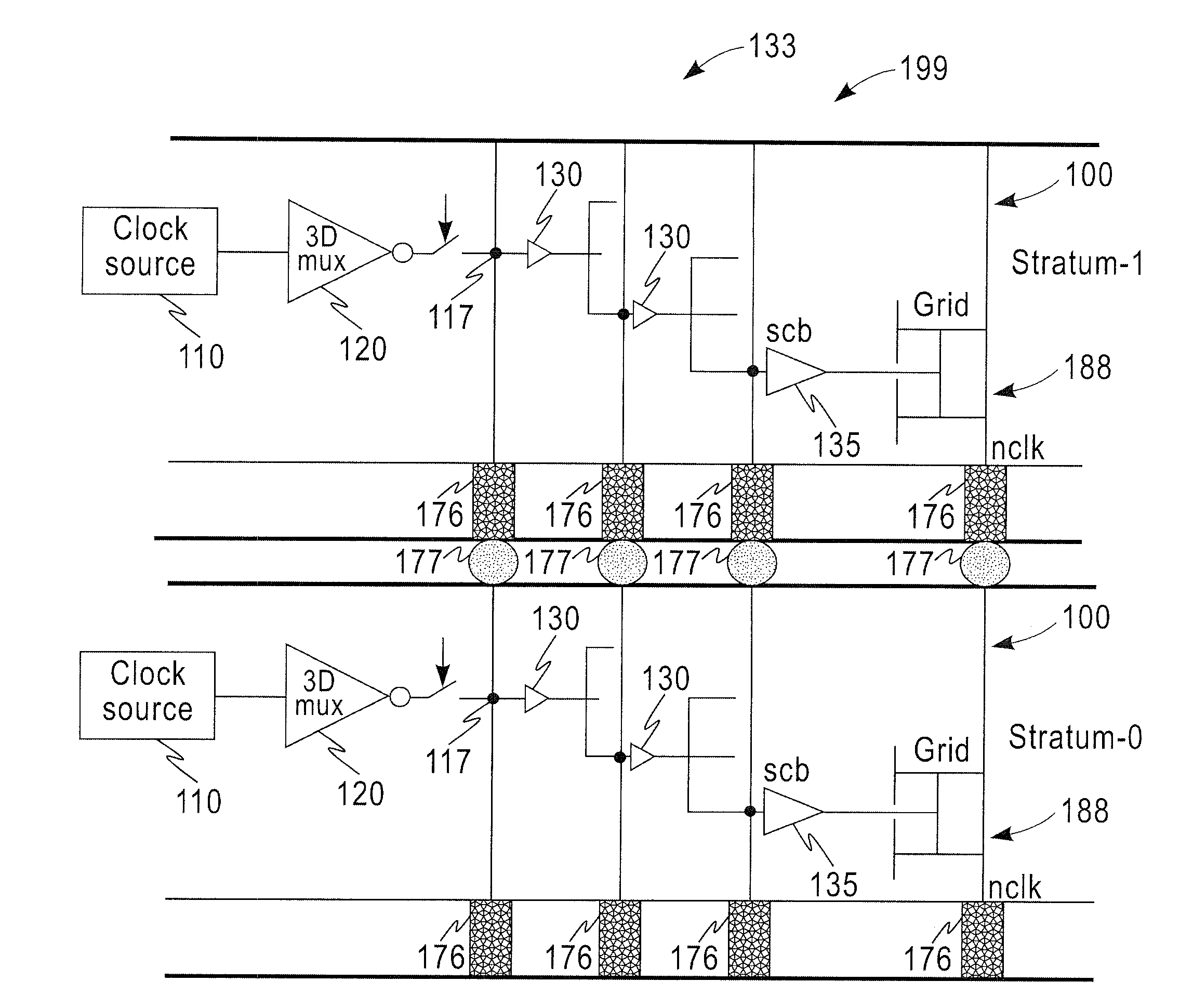
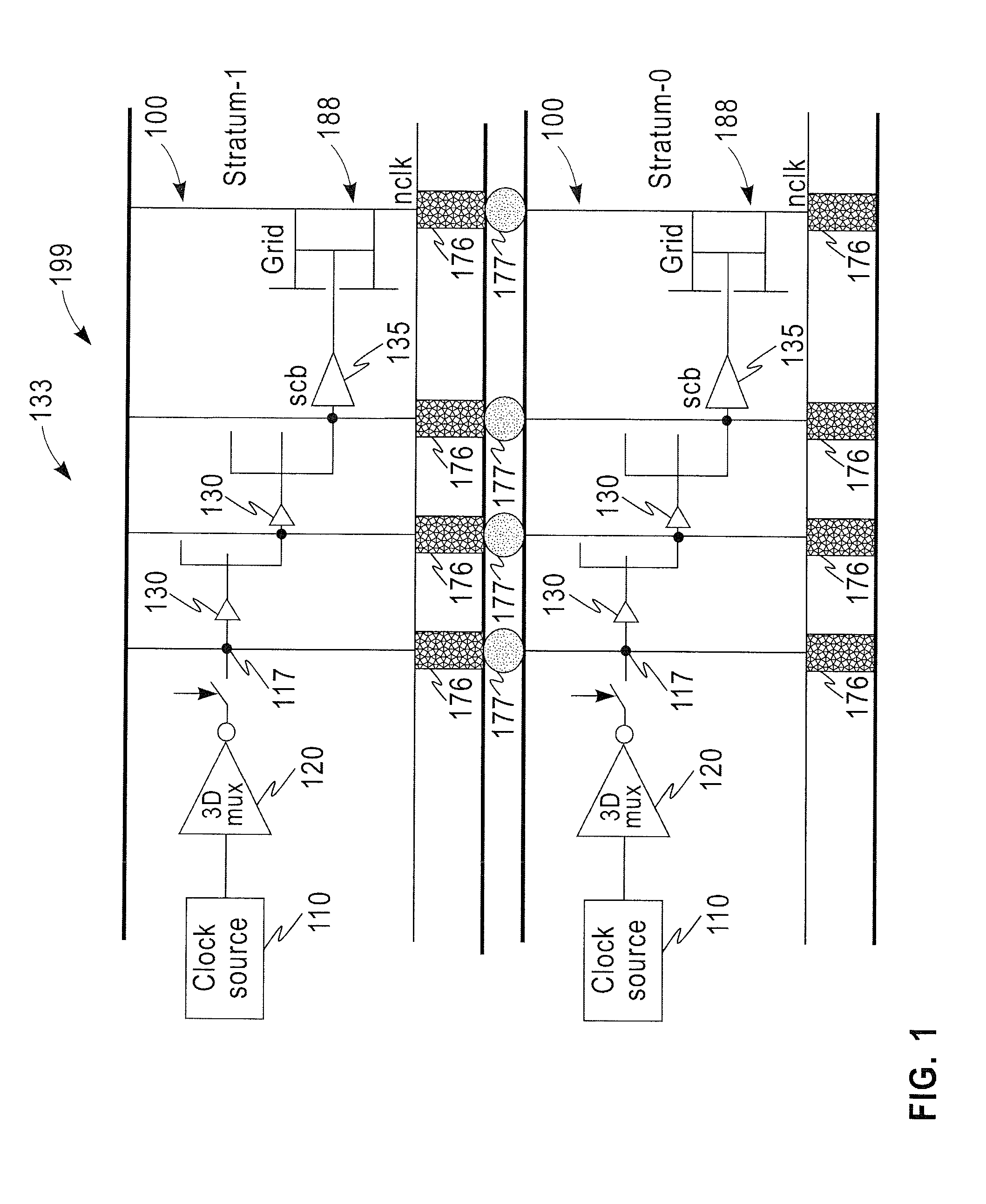
[0027]FIG. 1 shows a clock distribution network 133 for a 3D chip stack 199, in accordance with an embodiment of the present principles. The clock distribution network 133 includes shorted clock trees 100. Each stratum of the stack 199 includes a respective one of the shorted clock trees 100. Stack 199 includes a stratum-0 and a stratum-1.

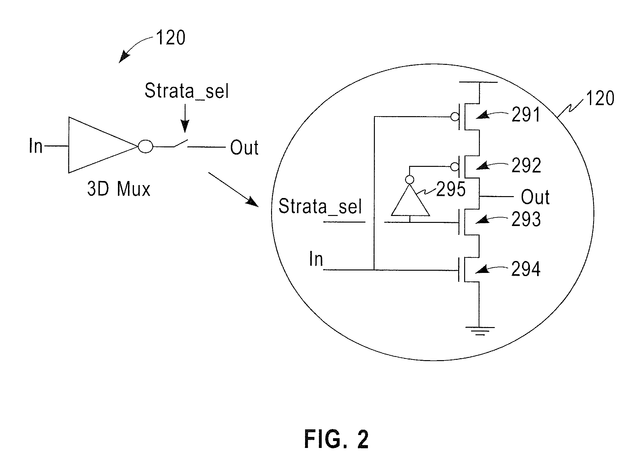
[0028]The shorted clock trees 100 have a single clock source 110 (e.g., a phase locked loop (PLL)), selectable using a 3D mux 120, for driving the root 117 of the clock trees in all strata. Clock buffers 130 on all strata are shorted together using through-Silicon vias (TSVs) 176 and micro C4 connections (μC4) 177. Inputs of the clock buffers 130 in the trees 100 are shorted, and uniform shorting is applied over the entire final clock mesh (nclk) 188. We note that the “final clock mesh” is interchangeably re...


PUM


Abstract

There is provided a clock distribution network for synchronizing global clock signals within a 3D chip stack having two or more strata. On each of the two or more strata, the clock distribution network includes a clock grid having a plurality of sectors for providing the global clock signals to various chip locations, a multiple-level buffered clock tree for driving the clock grid and including at least a root and a plurality of clock buffers, and one or more multiplexers for providing the global clock signals to at least a portion of the buffered clock tree. Inputs of at least some of the plurality of clock buffers on each of the two or more strata are shorted together using chip-to-chip interconnects to reduce skewing of the global clock signals with respect to the various chip locations.

Description

GOVERNMENT RIGHTS[0001]This invention was made with Government support under Contract No.: H98230-07-C-0409 (National Security Agency). The Government has certain rights in this invention.CROSS-REFERENCE TO RELATED APPLICATIONS[0002]This application is related to the following commonly assigned applications, all filed on Aug. 25, 2011 and incorporated herein by reference: U.S. patent application Ser. No. 13 / 217,734, entitled “PROGRAMMING THE BEHAVIOR OF INDIVIDUAL CHIPS OR STRATA IN A 3D STACK OF INTEGRATED CIRCUITS”; U.S. patent application Ser. No. 13 / 217,349, entitled “3D CHIP STACK SKEW REDUCTION WITH RESONANT CLOCK AND INDUCTIVE COUPLING”; U.S. patent application Ser. No. 13 / 217,767, entitled “3D INTEGRATED CIRCUIT STACK-WIDE SYNCHRONIZATION CIRCUIT”; U.S. patent application Ser. No. 13 / 217,789, entitled “CONFIGURATION OF CONNECTIONS IN A 3D STACK OF INTEGRATED CIRCUITS”; U.S. patent application Ser. No. 13 / 217,381, entitled “3D INTER-STRATUM CONNECTIVITY ROBUSTNESS”; U.S. pate...

Claims


Application Information

Patent Timeline
Patent Type & Authority Patents(United States)
IPC IPC(8): G06F1/04
CPCG06F1/10H01L24/16H01L24/94H01L25/0657H01L2224/16145H01L2224/94H01L2924/10252H01L2924/10253H01L2924/10329H01L2924/14H01L2924/1531H01L2225/06513H01L2225/06541H01L2225/06531H01L2224/81H01L2924/13091H01L2924/00
Inventor BUCELOT, THOMAS J.PANG, LIANG-TECKRESTLE, PHILLIP J.
Owner GLOBALFOUNDRIES US INC
Why Eureka
Try Eureka