Optimizing IC clock structures by minimizing clock uncertainty

a clock structure and uncertainty technology, applied in the direction of program control, generating/distributing signals, instruments, etc., can solve the problems of increasing the power consumption of the integrated circuit, difficult to implement clock logic changes without, and difficult to place buffers and route clock nets simultaneously, so as to reduce estimation errors and efficient computation and memory usage

Active Publication Date: 2006-08-22
BELL SEMICON LLC
View PDF64 Cites 17 Cited by
  • Summary
  • Abstract
  • Description
  • Claims
  • Application Information

AI Technical Summary

Benefits of technology

[0009]The present invention is directed to a technique for an early estimation of clock delay, and for reduction of estimation errors. The technique is useful in design optimization tools, and because delay changes dynamically during the optimization process, the developed technique is efficient in computation and memory usage.
[0013]In some embodiments, buffer placement to the clock net is optimized by forcing a buffer to the center of gravity of a plurality of inserted buffers driving respective clock nets without timing violations. The path between the root and the forced buffer defines a common path of maximum length to the leaves so that the non-common paths between the inserted buffer and the leaves is minimized, thereby minimizing clock uncertainty.

Problems solved by technology

However, each added buffer increases power consumption of the integrated circuit.
If a clock network is implemented after detailed routing, it is difficult to implement clock logic changes without changing the placement and the routing of data logics.
It is also difficult to place the buffers and route the clock nets simultaneously in order to take into account the coupling and other detailed information of the chip fabrication and materials (“silicon information”).
A mis-estimation of clock delays may cause thousands or more violated timing paths, and attempts to correct a poorly routed clock net may inadvertently cause other timing violations.
A calculated clock delay will unavoidably have estimation errors.
However, a conservative clock uncertainty value leads to other problems, such as adding unnecessary buffers to fix timing violations.

Method used


Image

  • Optimizing IC clock structures by minimizing clock uncertainty
  • Optimizing IC clock structures by minimizing clock uncertainty
  • Optimizing IC clock structures by minimizing clock uncertainty

Examples


Embodiment Construction

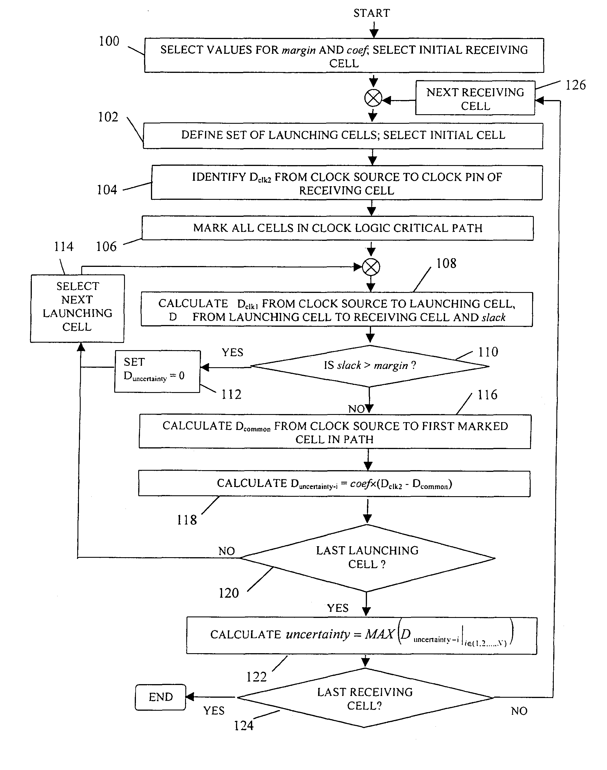
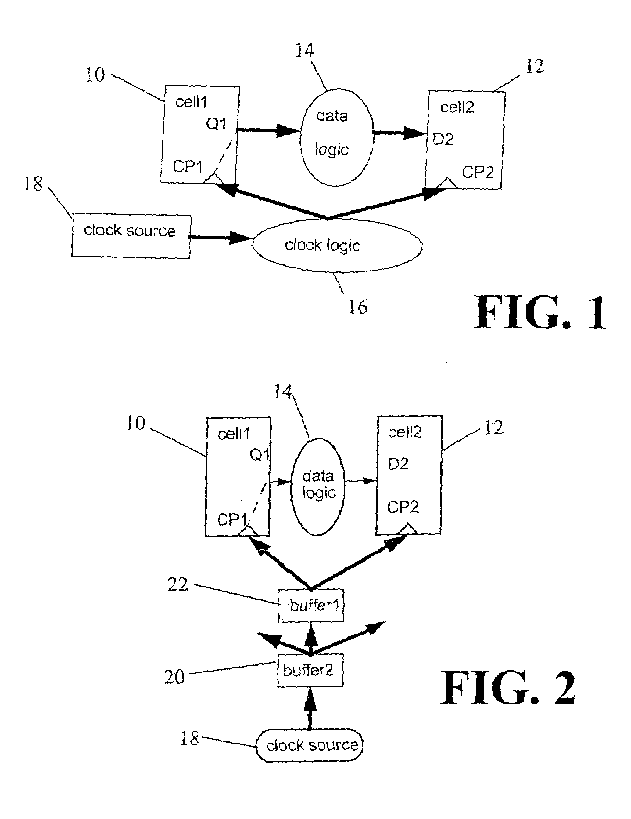
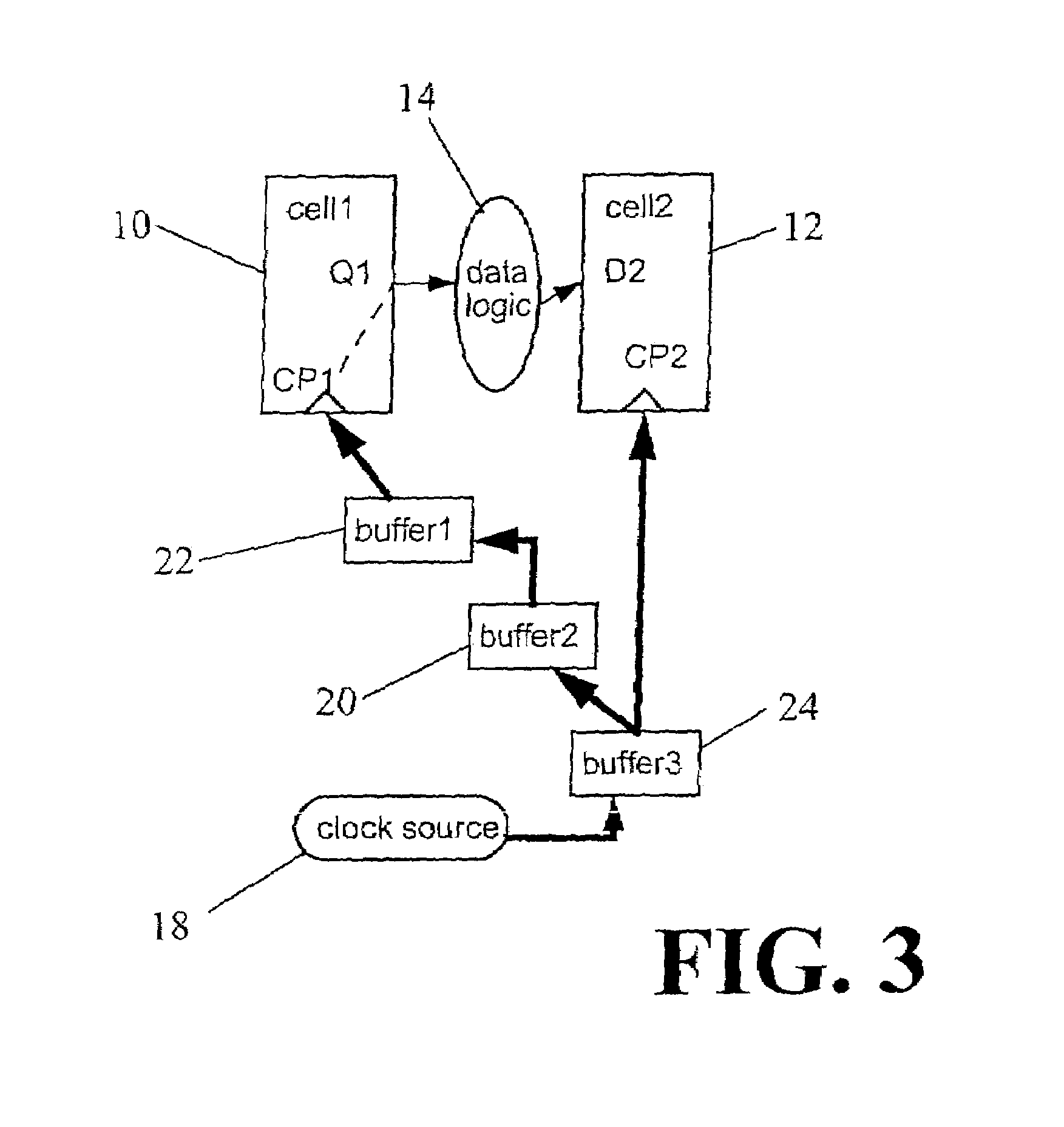
[0019]FIG. 1 illustrates a portion of an integrated circuit design having two sequential cells 10 and 12, data logics 14 and clock logics 16. If the circuit operates at frequency 400 MHz, the clock cycle, T, is 2.5 ns (nanoseconds) . The data path delay, Ddata, is the delay from clock pin CP1 in cell 10, through pin Q1 in cell 10 and data logic 14, to data pin D2 in cell 12. Clock delay, Dclk2, is the delay from clock source 18, though clock logic 16, to clock pin CP1, and clock delay, Dclk2, is the delay from clock source 18, through clock logic 16, to clock pin CP2. If

Dclk1+Ddata+setup+uncertainty−Dclk2>T,  (1)

where setup is a constant dependent on the technology and cell type, then the path ending at pin D2 has a timing violation. In other words, this design cannot work at the frequency of 400 MHz (but might operate at a lower frequency).

[0020]The value of uncertainty represents the maximal clock delay estimation errors. (As mentioned above, the clock delay estimation at the p...


PUM


Abstract

Clock uncertainty between a receiving cell and a launching cell of a net is estimated by back-tracing a first path from the receiving cell toward the clock source and marking each cell having a predetermined characteristic along the first path. A second path from the launching cell toward the clock source is back-traced to a common one of the marked cells having the predetermined characteristic. Clock uncertainty is calculated based on the portion of the first path from the common marked cell having the predetermined characteristic to the receiving cell. Clock uncertainty is calculated if a slack does not exceed a margin value. In one embodiment, a clock net in the form of a tree is optimized by forcing a first buffer to the center of gravity of a plurality of buffers having nets without timing violations to maximize a common path from the root to the forced buffer and minimize the non-common paths from the forced buffer to the leaves, thereby minimizing clock uncertainty.

Description

FIELD OF THE INVENTION[0001]This invention relates to designing clock logics in integrated circuits or chips, and particularly to optimizing clock logics during the design phase by minimizing clock uncertainty.BACKGROUND OF THE INVENTION[0002]Integrated circuits (ICs) comprise a large number of circuit elements, such as transistors, interconnected by a large number of wires. Some elements (“drivers”) drive other elements (“driven elements”). Fanout of a given driver is the number of driven elements coupled to the output of the driver.[0003]The “ramptime” of a driven element is the time required to drive a driven element to operation. Ramptime depends on the amount of capacitance and resistance “seen” by the driver, which in turn depends on the number of driven elements connected to the output of the driver and the length of the wires that interconnect the driver with its driven elements. If a driver's load exceeds a design threshold, the ramptime for the driven elements will also ex...

Claims


Application Information

Patent Timeline
Patent Type & Authority Patents(United States)
IPC IPC(8): G06F17/50G06F19/00G01R31/30G06F1/10G06F9/45
CPCG06F1/10G01R31/3016
Inventor LU, AIGUOPAVISIC, IVANRADOVANOVIC, NIKOLA
Owner BELL SEMICON LLC
Why Eureka
Try Eureka