Clock distribution circuit, semiconductor integrated circuit and method of designing clock distribution circuit

Inactive Publication Date: 2007-12-13
RENESAS ELECTRONICS CORP
View PDF5 Cites 18 Cited by
  • Summary
  • Abstract
  • Description
  • Claims
  • Application Information

AI Technical Summary

Benefits of technology

[0012]In the circuit thus configured, the first feedback clock signal is fed back from the first branch node, and the second feedback clock signal is fed back from the second branch node. Here, the first branch node is between the first PLL circuit and the first sequential circuit. The second branch node is between the second PLL circuit and the second sequential circuit. That is to say, the first feedback clock signal reflects a delay of the first clock signal at the first sequential circuit. The second feedback clock signal reflects a delay of the second clock signal at the second sequential circuit. It is therefore possible to make the delay of the

Problems solved by technology

As a result, the data transfer between the macro 3a and

Method used


Image

  • Clock distribution circuit, semiconductor integrated circuit and method of designing clock distribution circuit
  • Clock distribution circuit, semiconductor integrated circuit and method of designing clock distribution circuit
  • Clock distribution circuit, semiconductor integrated circuit and method of designing clock distribution circuit

Examples


first embodiment

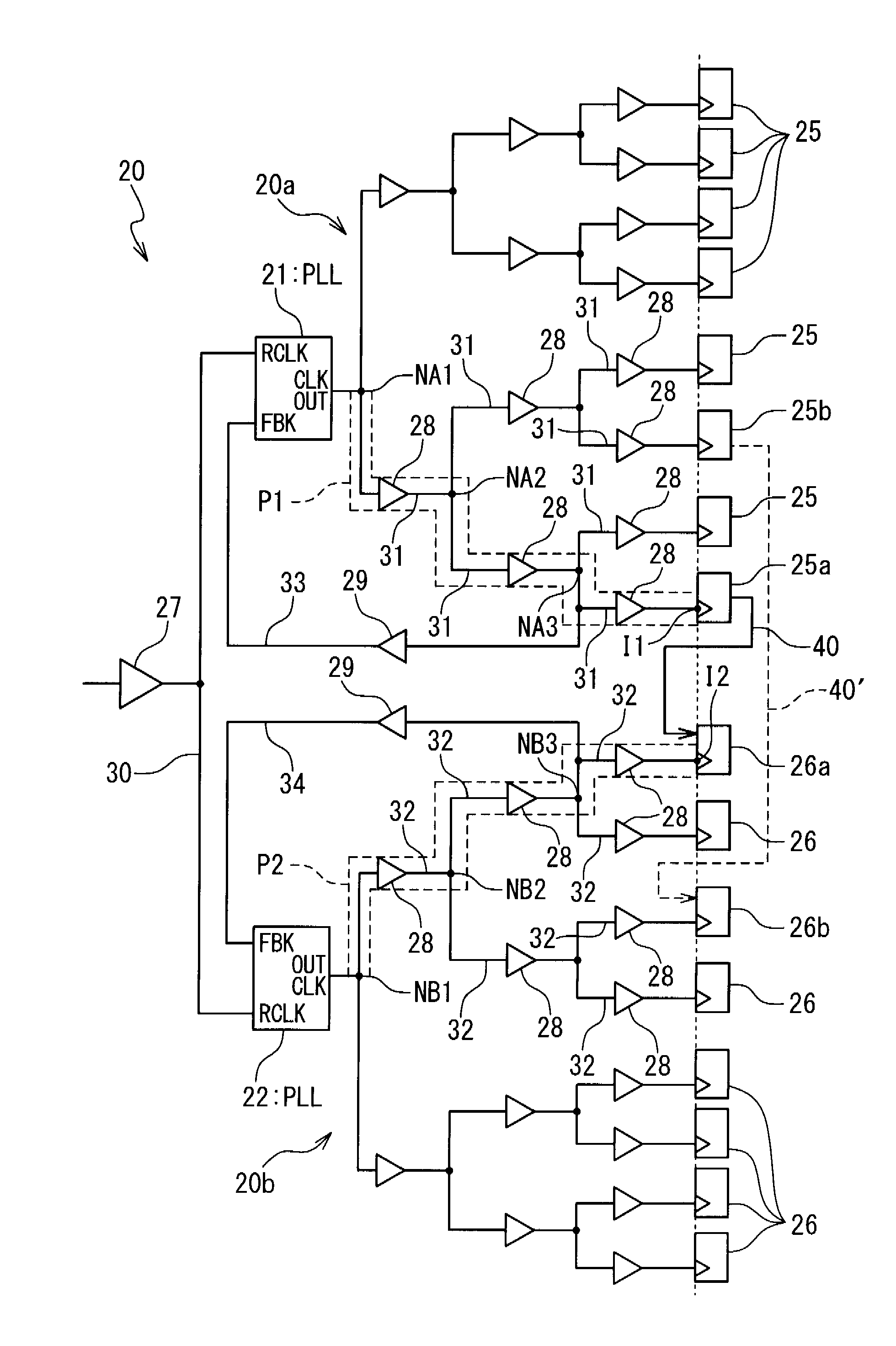
[0025]First, a clock distribution circuit according to the embodiment will be described. FIG. 2 is an equivalent circuit diagram showing a configuration of the clock distribution circuit according to the embodiment. The clock distribution circuit 20 is provided in a semiconductor integrated circuit (45: described later) and distributes a clock signal, which is generated by using frequency and phase of an external clock signal as a reference signal, to a plurality of sequential circuits 25, 25a, 25b, 26, 26a and 26b. Here, the sequential circuit 25a and the sequential circuit 26a are connected to each other through a data transfer path 40. That is, the data transfer path 40 is the “inter-domain data transfer path”. The clock distribution circuit 20 includes a clock distribution network 20a, a PLL circuit 21, a clock distribution network 20b, a PLL circuit 22, a clock driver 27 and an interconnection 30. In the present embodiment, a reference clock input from the outside is supplied f...

second embodiment

[0045]The phase of the first clock signal at the clock input terminal I1 of the sequential circuit 25a and the phase of the second clock signal at the clock input terminal I2 of the sequential circuit 26a are in synchronization with the phase of the external clock signal input to the clock input buffer 27. For example, the following configuration is provided in addition to the above-described configuration of the clock distribution circuit. That is, a buffer or an interconnection or both which has a delay time corresponding to the delay time of the clock input buffer 27 (to be precise, a delay time from an external clock input terminal (not shown) to the PLL circuits 21 and 22 through the clock input buffer 27) is added to the clock path from the branch node NA3 to the feedback clock terminal FBK of the PLL circuit 21 and the clock path from the branch node NB3 to the feedback clock terminal FBK of the PLL circuit 22. The other configuration is the same as that in the first embodime...

third embodiment

[0046]In the above-described first embodiment, the same reference clock signal is supplied to the PLL circuit 21 and the PLL circuit 22 (the second reference clock signal=the first reference clock signal). However, the present invention is not limited to that. The second reference clock signal and the first reference clock signal can be different reference clock signals, as long as they have a phase relationship that is known and is not changed. For example, when the frequency of one reference clock signal is constant times the frequency of the other reference clock signal, the risings of the clocks align with each other when the phases match. Such a relationship is also possible, as long as the phase relationship between the clock risings is known and is not changed.

[0047]Therefore, for example, a configuration that the clocks are supplied to the PLL circuits 21 and 22 through respective clock input buffers 27 is possible.

[0048]Moreover, the present invention can have a configurati...


PUM


Abstract

A clock distribution circuit, which is provided in IC that has a first sequential circuit receiving first clock through a first branch node on a first clock network, a second sequential circuit receiving second clock through a second branch node on a second clock network, and a data transfer path between the first and second sequential circuits, includes: a first PLL receiving a first feedback clock that is the first clock branched at the first branch node and outputting the first clock to the first clock network based on the first feedback clock; and a second PLL receiving a second feedback clock that is the second clock branched at the second branch node and outputting the second clock to the second clock network based on the second feedback clock. A branch node is provided at least one of between the first PLL and the first branch node and between the second PLL and the second branch node.

Description

BACKGROUND OF THE INVENTION[0001]1. Field of the Invention[0002]The present invention relates to a clock distribution circuit, a semiconductor integrated circuit, a method and a program for designing a clock distribution circuit.[0003]2. Description of Related Art[0004]A semiconductor integrated circuit (LSI) is provided with a clock distribution circuit that receives a clock from the outside and supplies the clock to a circuit requiring the clock in the semiconductor integrated circuit. The clock distribution circuit includes clock distribution interconnections and clock distribution buffers, and is configured such that clock distribution delay times from a clock supply source (clock source) to respective clock supply destinations (leafs) become uniform. A clock tree synthesis (CTS) method is used as a method for designing such the clock distribution circuit. The clock tree synthesis method has the following feature. That is, based on circuit connection information, placement infor...

Claims


Application Information

Patent Timeline
IPC IPC(8): H03D3/24
CPCG06F1/10
Inventor SHIMOBEPPU, MASAYUKI
Owner RENESAS ELECTRONICS CORP
Why Eureka
Try Eureka