Semiconductor integrated circuit

A technology of integrated circuits and semiconductors, applied in the direction of semiconductor devices, circuits, semiconductor/solid-state device components, etc., can solve the problems of increasing clock skew, different transistor delay characteristics, and different transistor characteristics, etc., to reduce clock offset effect

Inactive Publication Date: 2008-08-13
PANASONIC CORP
View PDF1 Cites 0 Cited by
  • Summary
  • Abstract
  • Description
  • Claims
  • Application Information

AI Technical Summary

Problems solved by technology

In the case of supplying a clock signal with CTS in a plurality of cell blocks having different cell heights, since transistors arranged in standard cells having different cell heights have different sizes, there is a problem that the characteristics of these transistors become different from each other. Same, with increased clock skew
[0015] For this reason, the problem that occurs in the conventional embodiment described in the above-mentioned Patent Document 1 is that due to the cell height of the standard cell, the distance between the diffusion regions in the standard cell, and the grid in the standard cell of different columns The distance between the electrodes is different, therefore, the delay characteristics of the transistors are different, and the clock skew increases

Method used


Image

  • Semiconductor integrated circuit
  • Semiconductor integrated circuit
  • Semiconductor integrated circuit

Examples


Embodiment 1

[0047] 7 is a plan view of a design example of a standard cell semiconductor integrated circuit according to Embodiment 1 of the present invention.

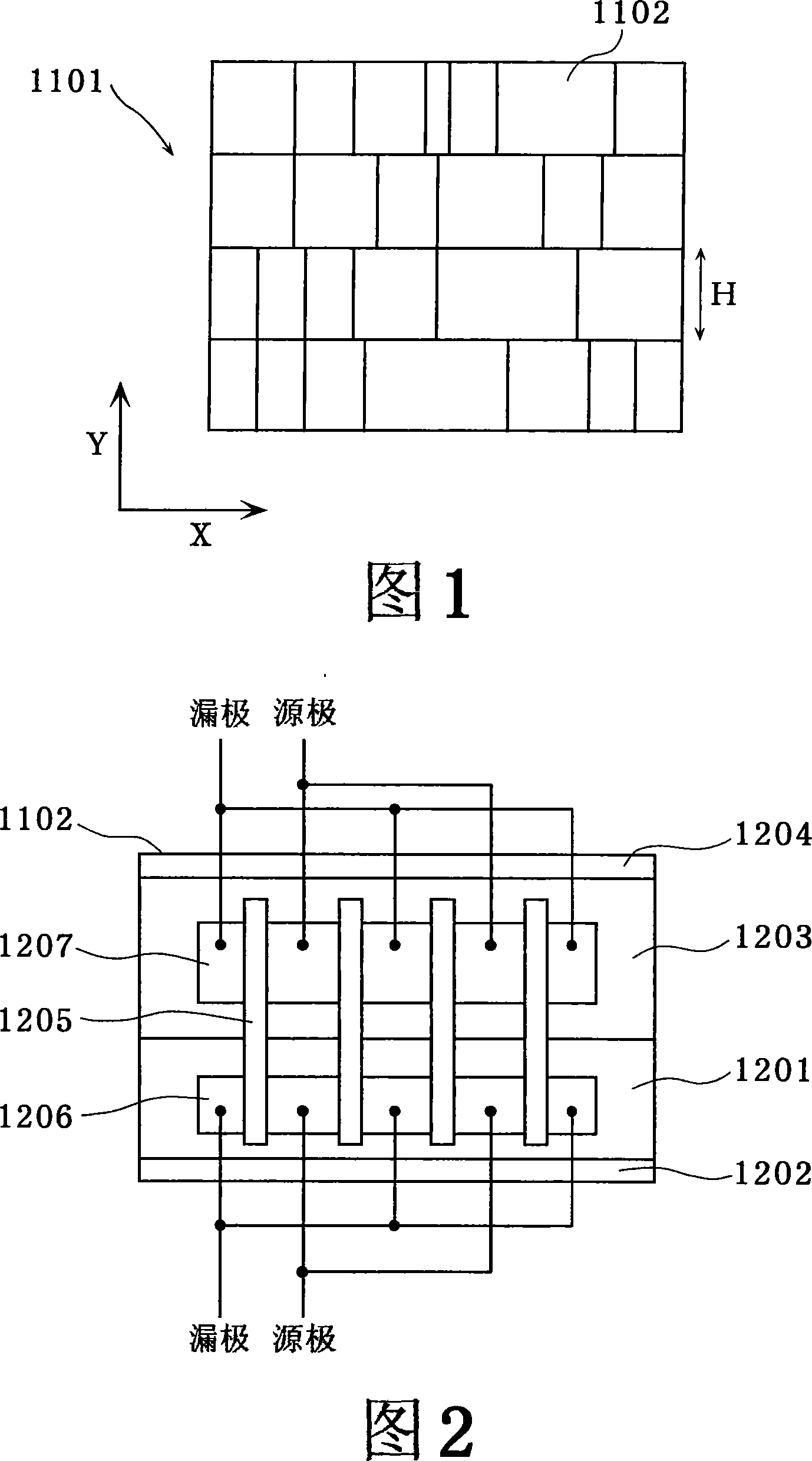
[0048] Four unit blocks 101 to 104 are shown in FIG. 7 . Each of the cell blocks 101 to 104 has a plurality of columns of standard cells, and in these columns of standard cells, a plurality of standard cells 105 to 110 are arranged in the direction of the columns. In addition, a plurality of standard cells 105 and 109 having low cell heights are arranged in the cell block 101 . A plurality of standard cells 106 and 110 having a higher cell height than standard cells 105 and 109 in the cell block 101 are arranged in the cell block 102 . A plurality of standard cells 107 and 108 having a low cell height are arranged in the cell blocks 103 and 104 , and the cell height of the plurality of standard cells 107 and 108 is the same as that of the standard cell 105 in the cell block 101 .

[0049] Moreover, the column directions of all ...

Embodiment 2

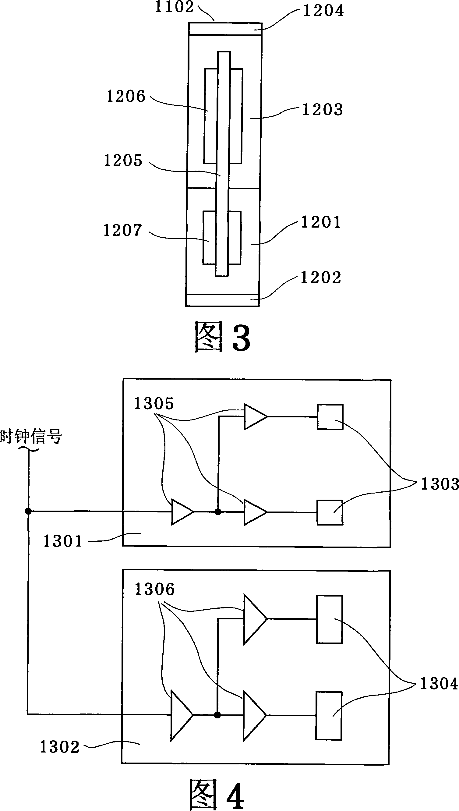
[0064] 11A and 11B are layout diagrams of clock standard cells in the semiconductor integrated circuit according to the second embodiment of the present invention. FIG. 11A is a schematic diagram of a standard cell 109 in the cell block 101 in FIG. 7 , and FIG. 11B is a schematic diagram of a standard cell 110 in the cell block 102 in FIG. 7 . In addition, in FIGS. 11A and 11B , parts corresponding to those in FIGS. 8A and 8B are assigned the same reference numerals, and description thereof will be omitted here. FIGS. 11A and 11B are the same as FIGS. 8A and 8B , showing an example in which the standard cells 109 and 110 are inverting cells as represented by the circuit of FIG. 9 .

[0065] The metal wiring 401 of the first metal wiring layer is shown in FIGS. 11A and 11B . In FIGS. 11A and 11B , the source 501 of the N-channel transistor 203 is connected to the P-type diffusion region 207 for providing substrate power through the contact 402 and the metal wiring 401 of the f...

Embodiment 3

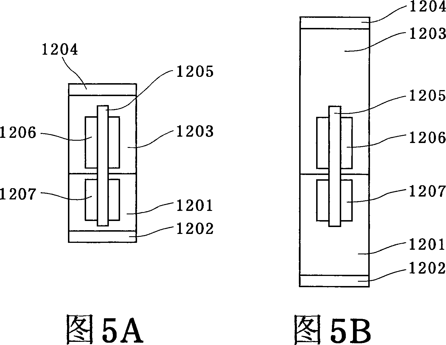
[0076] 13A and 13B are layout diagrams of clock standard cells in the semiconductor integrated circuit according to Embodiment 3 of the present invention. In addition, in FIGS. 13A and 13B , parts corresponding to those in FIGS. 8A and 8B are denoted by the same reference numerals, and description thereof will be omitted here. FIGS. 13A and 13B are the same as FIGS. 8A and 8B , and the standard cell shows an example of the inverting cell represented by the circuit of FIG. 9 .

[0077] The cell height of the standard cell 702 of FIG. 13B is higher than that of the standard cell 701 of FIG. 13A . Furthermore, in standard cell 702 in FIG. 13B , dummy gate wiring 703 is arranged on P well region 201 and N well region 202 , respectively. And, the distance 705 in the gate length direction between the gate electrode 209 in the standard cell 702 and the dummy gate wiring 703 is twice the distance 704, which is the distance 704 between the gate electrode 209 and the standard cell boun...


PUM


Abstract

An object of the present invention is to provide a semiconductor integrated circuit including a plurality of cell blocks respectively configured with standard cells having different cell heights and capable of reducing clock skew between the cell blocks, the semiconductor integrated circuit comprising A first standard cell and a second standard cell different in cell height from the first standard cell, a pair of N-type diffusion regions and a first substrate for providing the first standard cell are arranged in the P well region of the first standard cell The P-type diffusion region of the power supply, a pair of N-type diffusion regions and the P-type diffusion region for providing the second substrate power supply to the second standard cell are arranged in the P well region of the second standard cell, and the N-type diffusion region of the first standard cell The distance between the N-type diffusion region and the P-type diffusion region is substantially the same as the distance between the N-type diffusion region and the P-type diffusion region of the second standard cell.

Description

technical field [0001] The present invention relates to a standard cell type semiconductor integrated circuit in which standard cells having different cell heights are mixed. Background technique [0002] In a standard cell type semiconductor integrated circuit, generally, the height of each cell (cell height) is designed to be uniform, as shown in FIG. 1 , in order to arrange standard cells at high density without voids. FIG. 1 shows a plan view of a design example of a cell block 1101 including standard cells 1102 of a plurality of columns (four columns in FIG. 1 ). Here, the cell height of each standard cell 1102 refers to the height of the standard cell 1102 in the direction (Y-axis direction in FIG. 1 ) perpendicular to the column direction (X-axis direction in FIG. 1 ), which is the direction in which the standard cells 1102 are arranged. The dimensions of the unit, the height of this unit is represented by the symbol H in Figure 1. [0003] When aiming at high integ...

Claims


Application Information

Patent Timeline
Patent Type & Authority Applications(China)
IPC IPC(8): H01L27/02H01L23/528
CPCH01L27/0207H01L27/11807
Inventor 农添三资
Owner PANASONIC CORP
Why Eureka
Try Eureka