Liquid crystal display device

Active Publication Date: 2011-03-10
PANASONIC LIQUID CRYSTAL DISPLAY CO LTD +1
View PDF5 Cites 38 Cited by
  • Summary
  • Abstract
  • Description
  • Claims
  • Application Information

AI Technical Summary

Benefits of technology

[0021]According to the present invention, it is possible to apply an IPS method which is characterized by a large field of view and large transmissivity to a miniaturized and high-pixel-definition liquid crystal display device. To be more specific, the present invention can prevent the peeling-off betw

Problems solved by technology

The IPS-type liquid crystal display device differs from a conventional TN-type liquid crystal display device or the like in structure and hence, in the miniaturization of the liquid crystal display device or the reduction of thickness of the liquid crystal display device, there arise drawbacks in the IPS-type liquid crystal display device which differ from drawbacks that the conventional TN-type liquid crystal display device or the like has.
To the

Method used


Image

  • Liquid crystal display device
  • Liquid crystal display device
  • Liquid crystal display device

Examples


embodiment 1

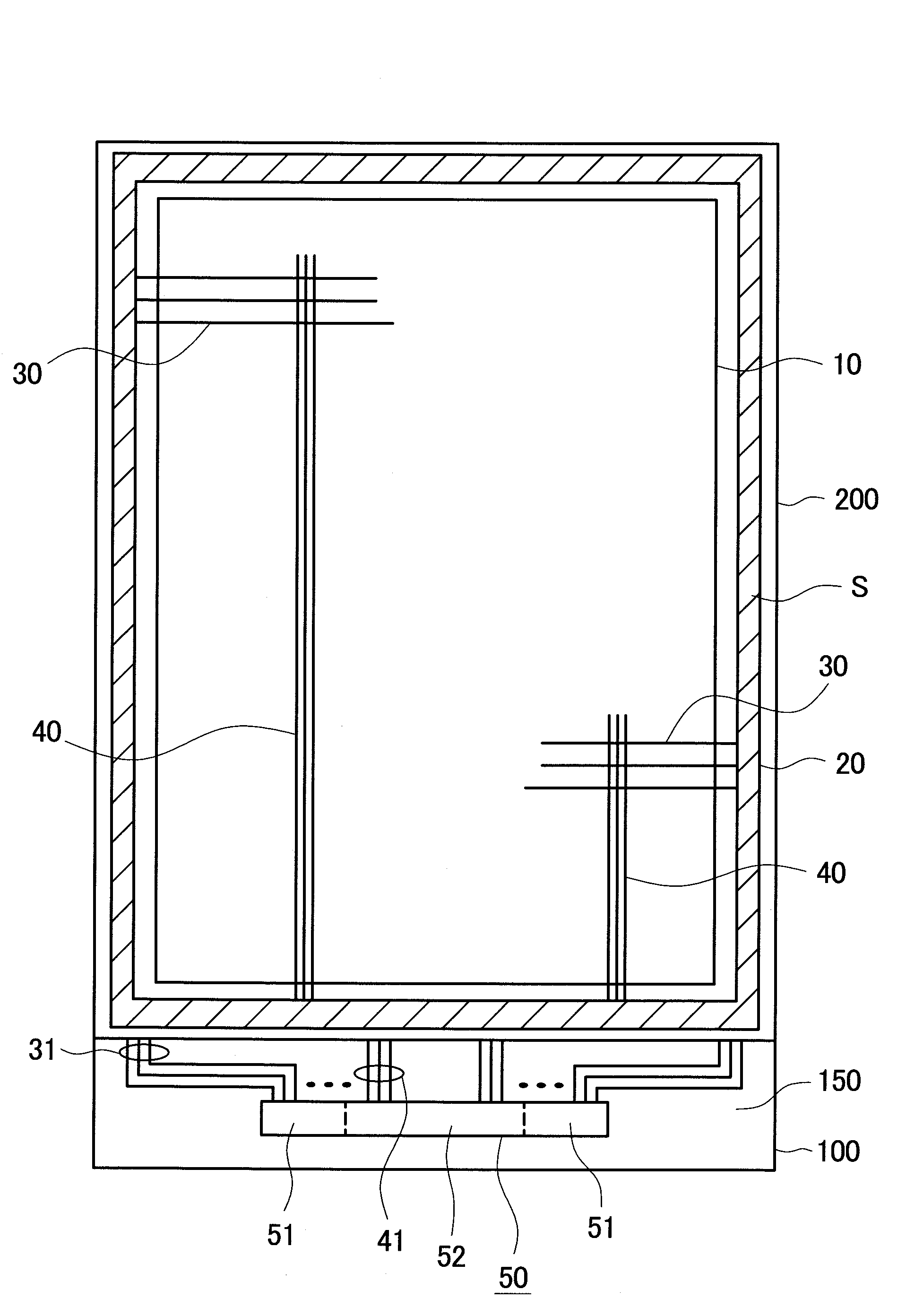
[0038]FIG. 1 is a plan view of a miniaturized liquid crystal display device used in a mobile phone or the like which is an example of a product to which the present invention is applied. In FIG. 1, a counter substrate 200 is arranged over the TFT substrate 100. A liquid crystal layer not shown in the drawing is sandwiched between the TFT substrate 100 and the counter substrate 200. The TFT substrate 100 and the counter substrate 200 are adhered to each other by a sealing material 20 which is formed between picture frame portions of these substrates. In FIG. 1, liquid crystal is sealed by a dropping method and hence, a sealing hole is not formed.

[0039]The TFT substrate 100 is formed larger than the counter substrate 200 in size. On a portion of the TFT substrate 100 projecting from the counter substrate 200, a terminal portion1150 for supplying a power source, a video signal, a scanning signal and the like to the liquid crystal cells is formed.

[0040]Further, an IC driver 50 for drivi...

embodiment 2

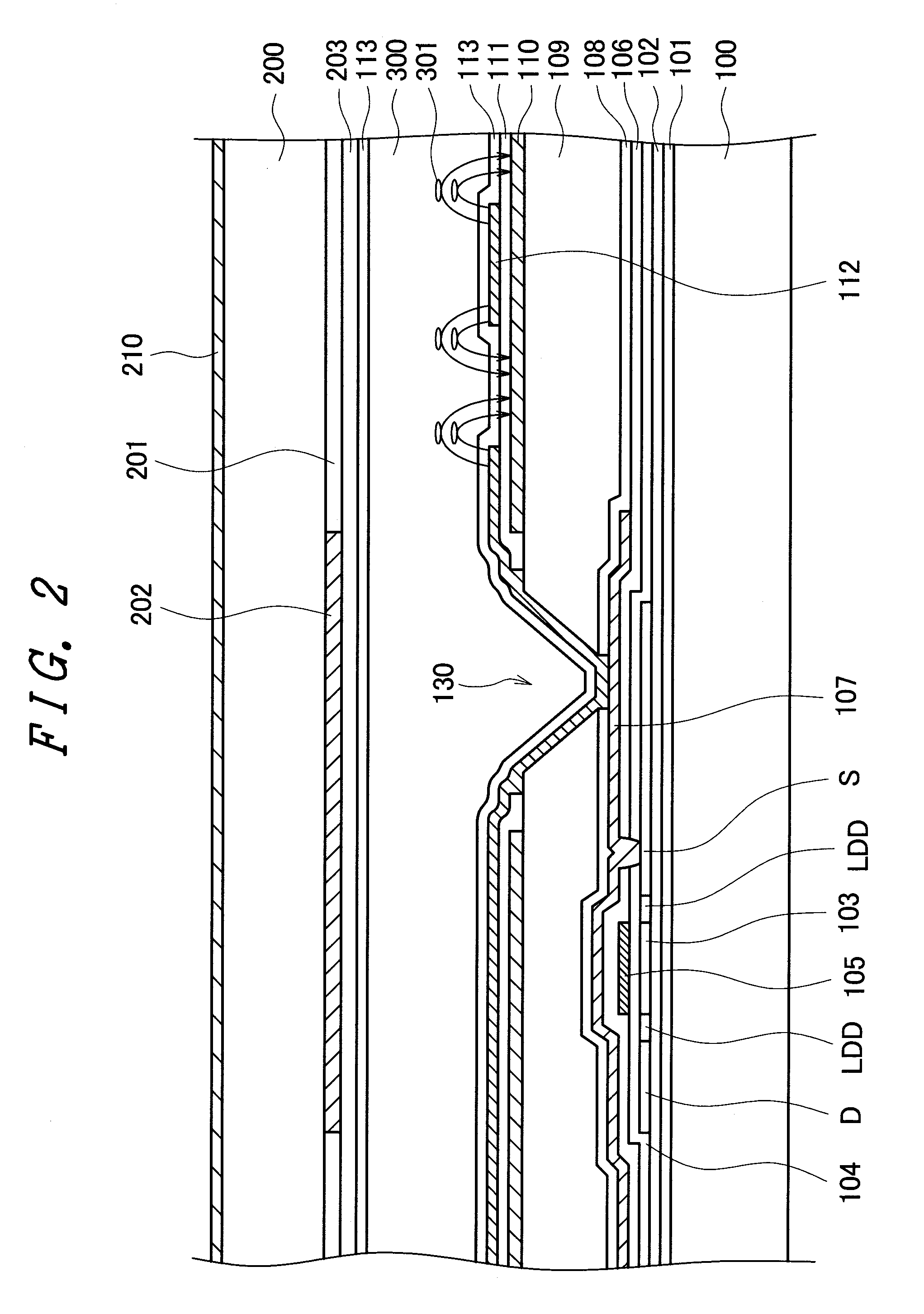
[0078]FIG. 12 is a plan view of an area in the vicinity of a through hole 130 in the embodiment 2. FIG. 12 differs from FIG. 4 showing the embodiment 1 only with respect to a range where an interlayer insulation film 111 is formed. That is, in this embodiment, the interlayer insulation film 111 covers a portion of an inclined portion of the through hole 130. FIG. 13 is a cross-sectional view taken along a line C-C in FIG. 12. In FIG. 13, the interlayer insulation film 111 covers an upper portion of the inclined portion of the through hole 130. However, the interlayer insulation film 111 does not extend to a lower portion of the through hole 130 and, at the same time, is not brought into contact with an inorganic passivation film 108.

[0079]Also in this embodiment, the inorganic passivation film 108 is etched by dry etching using an organic passivation film 109 as a mask and hence, the inorganic passivation film 108 does not appear on a surface. However, even if the inorganic passivat...

embodiment 3

[0083]The case in which the present invention adopts the top-gate-type TFT has been explained with respect to the embodiment 1 and the embodiment 2. However, the present invention is also applicable to a bottom-gate-type TFT in the same manner besides the top-gate-type TFT.

[0084]FIG. 14 is a cross-sectional view of the pixel portion when the present invention is applied to a liquid crystal display device which uses the bottom-gate-type TFT. Except for the constitution of the TFT, the constitution of the pixel portion in this embodiment is substantially equal to the constitution of the pixel portion shown in FIG. 2 explained in conjunction with the embodiment 1. In FIG. 14, a gate electrode 105 is formed on a TFT substrate 100. A gate insulation film 104 is formed so as to cover a gate electrode 105. A semiconductor layer 103 is formed over the gate electrode 105 by way of the gate insulation film 104.

[0085]In FIG. 14, the gate electrode 105 is directly formed on a glass substrate, a...


PUM


Abstract

In an IPS-type liquid crystal display device, peeling-off between a common electrode formed in a matted manner in plane and an interlayer insulation film is prevented. The common electrode is formed on an organic passivation film in a matted manner in plane, the interlayer insulation film is formed on the common electrode, and a comb-teeth-shaped pixel electrode is formed on the interlayer insulation film. The pixel electrode is connected with a source electrode via a through hole formed in the organic passivation film and an inorganic passivation film.

Description

CROSS-REFERENCE TO RELATED APPLICATION[0001]The present application claims priority from Japanese application JP 2009-208067 filed on Sep. 9, 2009, the content of which is hereby incorporated by reference into this application.BACKGROUND OF THE INVENTION[0002]The present invention relates to a display device, and more particularly to a lateral-electric-field liquid crystal display device which exhibits an excellent field-of-view characteristic and high reliability.[0003]In a liquid crystal display device, a TFT substrate on which pixels each of which includes a pixel electrode, a thin film transistor (TFT) and the like are formed in a matrix array and a counter substrate which faces the TFT substrate in an opposed manner and on which color filters are formed at positions corresponding to the pixel electrodes on the TFT substrate are arranged, and liquid crystal is sandwiched between the TFT substrate and the counter substrate. In the liquid crystal display device, an image is formed...

Claims


Application Information

Patent Timeline
IPC IPC(8): G02F1/1333
CPCG02F1/133345G02F1/136227G02F1/134363
Inventor ISHIGAKI, TOSHIMASATAKAHASHI, FUMIO
Owner PANASONIC LIQUID CRYSTAL DISPLAY CO LTD
Why Eureka
Try Eureka