Intergrated circuit (IC) with primary and secondary networks and device containing such IC

a technology of integrated circuits and networks, applied in the field of configurable integrated circuits, can solve the problems of less resources for implementing user designs, and more complicated debugging networks, and achieve the effect of halting the operation of the system

Active Publication Date: 2011-03-10
ALTERA CORP
View PDF99 Cites 44 Cited by
  • Summary
  • Abstract
  • Description
  • Claims
  • Application Information

AI Technical Summary

Benefits of technology

[0021]The configurable nature of the secondary circuit structure in some embodiments facilitates various overlay applications that operate in conjunction with the operation of the primary circuit structure in order to provide users with sophisticated debugging, diagnosing, and testing functionality that extend beyond traditional debug functionality of other ICs. One such overlay application of the secondary circuit structure is to monitor various tiles or circuits of the primary circuit structure in order to provide bandwidth measurements for these tiles or circuits. In this manner, the secondary circuit structure identifies bottlenecks within the primary logic functionality during runtime of the primary circuit structure without interfering with the runtime operation of the primary circuit structure.
[0022]Another example of an overlay application of the secondary circuit structure determines the usage of various resources within the primary circuit structure. For example, by monitoring buffers, memories, or queues (e.g., first in first out (FIFO) queue) of the primary circuit structure, some embodiments are able to determine a real-time state of the resources. Such functionality facilitates the detection of data overflows, data overwrites, or data corruption occurring within resources of the primary circuit structure.
[0024]In some embodiments, the secondary circuit structure modifies the operations of circuits of the primary circuit structures during operation of the primary circuit structure and without usurping resources of the primary circuit structure. For instance, in this manner, some embodiments allow designers the ability to test modifications to an adaptive filter or modify the operation of an adaptive filter using the secondary circuit structure based on perceived patterns. Moreover, the modifications may be made without modification to the configuration of the primary circuit structure, allowing the user design implemented by the primary logic to continue operating unhindered and unknowing of the changes occurring to the coefficients of the adaptive filter. Additionally, in some embodiments, the operations of the filter are modified by altering the configuration data used to configure the circuits implementing the filter.
[0025]In some embodiments, an overlay application of the secondary circuit structure secures the functionality of a system operating in conjunction with the primary circuit structure of the IC. In some such embodiments, the primary circuit structure of the IC provides various logic functionalities for the system and the secondary circuit structure secures the system by intercepting anomalous behavior that could otherwise cause the primary circuit structure or other system components to malfunction and thus halt operation of the system. The secondary circuit structure triggers an assertion upon detecting the anomalous behavior within the primary circuit structure. The assertion generates an interrupt that is detected by one or more components of the system with logic for modifying the operation of the system to correct or avoid processing the anomalous behavior.

Problems solved by technology

However, many such user designs include various design bugs, design defects, or unexpected runtime behavior that pass unseen through design and testing.
In such cases, a more complicated debug network consumes greater resources of the IC, leaving fewer resources for implementing the user design.
As a result, user designs become less sophisticated.
Additionally, a change to either the core logic functionality of the primary network or the functionality of the debug network could cause the entire IC design to have to be recompiled, downloaded, and loaded onto the IC.
This is due to the fact that changes to a design, even when made on a small scale to localized circuits, could have a design-wide impact affecting the overall circuit routing or timing of the design.
These changes also create the risk that the circuit logic, including seemingly unrelated logic, may be “broken” due to errors in implementing the new functional change.
Because of this risk, extensive regression testing and verification of the logic of the primary network and debug network is required.
However, implementing the debugging circuitry as fixed-function circuitry also has several drawbacks.
Therefore, the dedicated resources of the debug network go unused and are effectively wasted as these resources cannot be modified to complement the functionality of the primary network that implements the user design.
Unanticipated usage, behavior, or operating conditions in the field could pose issues beyond the debugging scope of the programmed debug network, forcing users to have to employ third party tools or other means to perform the additional debug functionality needed to handle the unanticipated usage, behavior, or operating conditions.

Method used


Image

  • Intergrated circuit (IC) with primary and secondary networks and device containing such IC
  • Intergrated circuit (IC) with primary and secondary networks and device containing such IC
  • Intergrated circuit (IC) with primary and secondary networks and device containing such IC

Examples


Embodiment Construction

[0094]In the following detailed description of the invention, numerous details, examples, and embodiments of the invention are set forth and described. However, it will be clear and apparent to one skilled in the art that the invention is not limited to the embodiments set forth and that the invention may be practiced without some of the specific details and examples discussed.

[0095]I. Overview

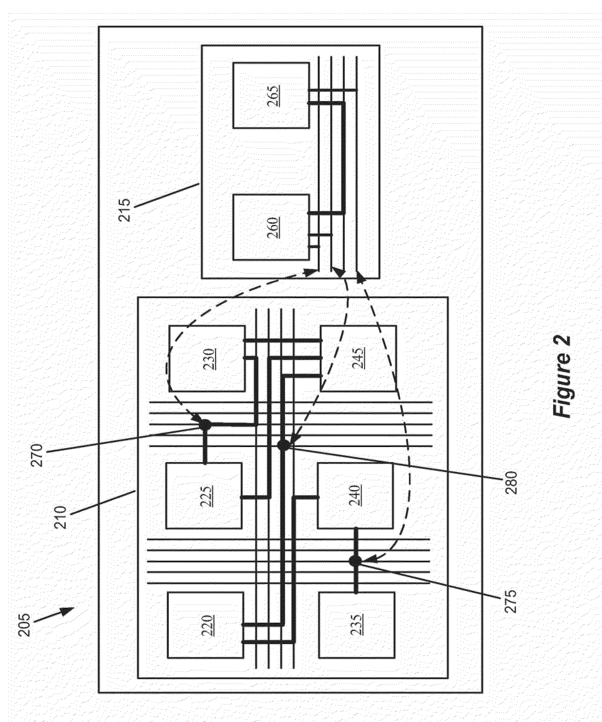
[0096]Some embodiments provide a single integrated circuit (“IC”) that includes (1) a primary circuit structure that implements a user design and (2) a secondary circuit structure that monitors the primary circuit structure by using a network and that performs one or more overlay applications based on the monitoring of the primary circuit structure. In some embodiments, the overlay functionality provided by the secondary circuit structure includes (1) monitoring the primary circuit structure in real-time, (2) monitoring raw data in the primary circuit structure to analyze performance of the pr...


PUM


Abstract

Some embodiments provide an integrated circuit (“IC”) with a primary circuit structure. The primary circuit structure is for performing multiple operations that implement a user design. The primary circuit structure includes multiple circuits. The IC also includes a secondary monitoring structure for monitoring multiple operations. The secondary monitoring structure includes a network communicatively coupled to multiple circuits of the primary circuit structure. The secondary monitoring circuit structure is for analyzing the monitored operations and reporting on the analysis to a circuit outside of the IC.

Description

CLAIM OF BENEFIT TO RELATED APPLICATIONS[0001]This application claims the benefit of U.S. Provisional Application 60 / 973,736, entitled “Overlay Applications for a Second Network of a Configurable IC,” filed Sep. 19, 2007; U.S. Provisional Application 61 / 042,695, entitled “Overlay Applications for a Secondary Network of a Configurable IC,” filed Apr. 4, 2008; U.S. Provisional Application 61 / 055,956, entitled “Overlay Applications for a Secondary Network of a Configurable IC,” filed May 23, 2008; and U.S. Provisional Application with Attorney Docket TBUL.P0111P, entitled “Trigger Circuits and Event Counters for a Monitoring Network of a Configurable IC,” concurrently filed Sep. 19, 2008. All of the above mentioned applications, namely 60 / 973,736, 61 / 042,695, 61 / 055,956, and TBUL.P0111P are incorporated herein by reference.FIELD OF THE INVENTION[0002]The field of invention relates generally to configurable integrated circuits. More particularly, this invention relates to methods and sy...

Claims


Application Information

Patent Timeline
Patent Type & Authority Applications(United States)
IPC IPC(8): G01R27/28
CPCG11C2029/0409G06F11/221G01R31/3177
Inventor MILLER, MARCTEIG, STEVENHUTCHINGS, BRADTHOM, DANNY
Owner ALTERA CORP
Why Eureka
Try Eureka