Magnetoresistive effect element in CPP structure and magnetic disk device
- Summary
- Abstract
- Description
- Claims
- Application Information
AI Technical Summary
Benefits of technology
Problems solved by technology
Method used
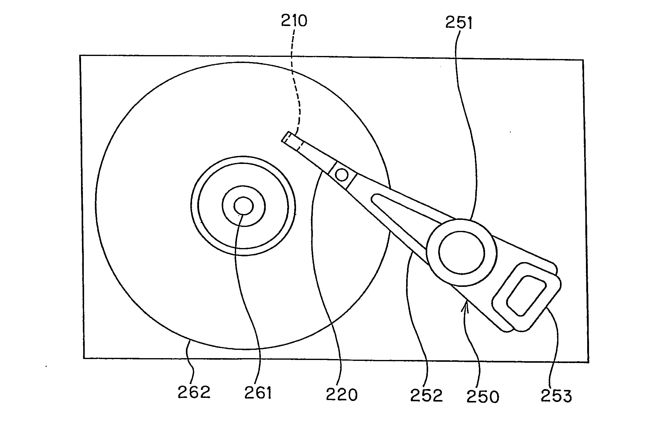
Image

Examples
embodiment 1
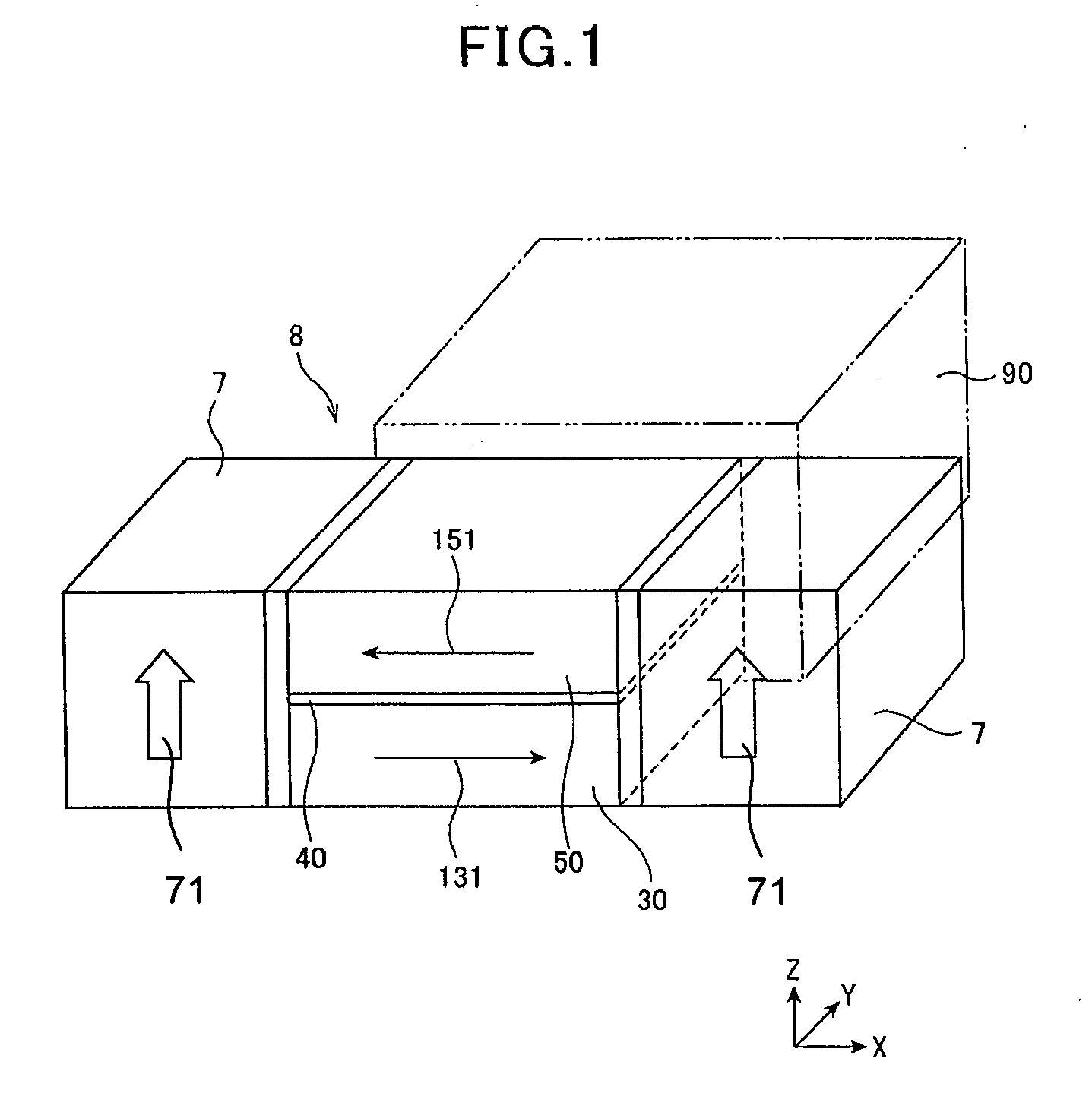
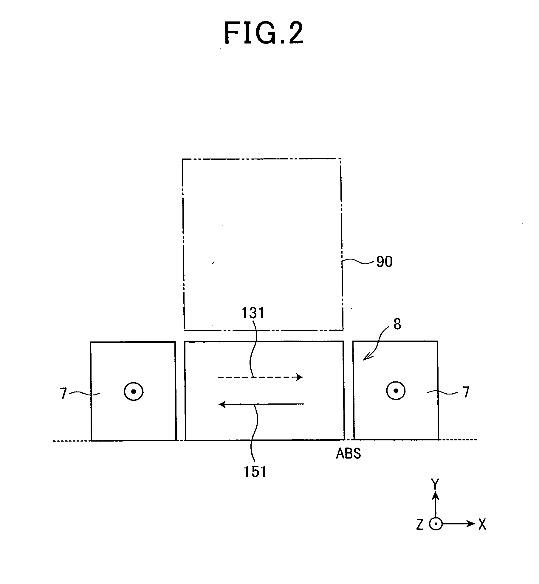
Fabrication for Embodiment 1 Sample
[0169]A MR effect layer, which functions as a DFL element and is configured with a lamination structure as shown in Table 1 below, was formed.
[0170]In the lamination structure of Table 1 below, a read gap length corresponding to a main part of the sensor is 14.6 nm that was a total layer thickness of the first antiferromagnetic coupling intermediate layer (300′), the first ferromagnetic layer (50), the nonmagnetic intermediate layer (40), the second ferromagnetic layer (30), and the second antiferromagnetic coupling intermediate layer (500′). After layers were formed, the lamination structure was processed by a heat treatment at 250° C. for three hours in a magnetic field of 1 tesla (T).
TABLE 1Layer Layer Lamination StructureMaterialThickness (nm)Upper Main Shield Layer (5a)NiFe1000Antiferromagnetic Layer (5b)IrMn7.0Upper Exchange-Coupling CoFe1.0Shield Layer (5c)NiFe8.0CoFe1.0Ru0.8CoFe1.0NiFe8.0CoFe1.0Second Antiferromagnetic CouplingRu0.8Intermed...
PUM
 Abstract
Description
Claims
Application Information
 - R&D Engineer
- R&D Manager
- IP Professional
- Industry Leading Data Capabilities
- Powerful AI technology
- Patent DNA Extraction
Browse by: Latest US Patents, China's latest patents, Technical Efficacy Thesaurus, Application Domain, Technology Topic.
© 2024 PatSnap. All rights reserved.Legal|Privacy policy|Modern Slavery Act Transparency Statement|Sitemap