Laminate, preparatory support, method for producing laminate, and method for producing device

a technology of laminate and support, which is applied in the direction of sustainable manufacturing/processing, final product manufacturing, transportation and packaging, etc., can solve the problems of chipping, difficulty in transporting the wafer, and difficulty in securing the uniformity

Active Publication Date: 2011-03-31
DAI NIPPON PRINTING CO LTD
View PDF17 Cites 51 Cited by
  • Summary
  • Abstract
  • Description
  • Claims
  • Application Information

AI Technical Summary

Benefits of technology

[0052]As described above, the laminate of the present invention can successfully produce a thin device element on a flexible substrate which is likely to bend or break.
[0053]The preparatory support of the present invention can provide the laminate which can successfully produce a thin device element on a flexible substrate which is likely to bend or break.
[0054]The laminate production method of the present invention can successfully produce a thin device element on a flexible substrate which is likely to bend or break.
[0055]Further, the device production method of the present invention can successfully produce a device comprising a flexible substrate which is likely to bend or break, and a thin device element formed on the substrate.

Problems solved by technology

Due to warpage of a wafer caused by thinning, however, such wafer thinning entails problems such as difficulty in securing the uniformity of thickness upon grinding of the wafer, difficulty in transporting the wafer, the occurrence of chipping (edge chipping) during dicing of the wafer into chips, etc.
Such a substrate of quartz glass or heat-resistance glass is fragile and heavy in weight, and therefore entails the problem of difficult handling upon the production of a large-sized LCD.
Thus, in the fields of semiconductor technology and LCD technology, in order to overcome the problems such as deflection or warpage of a wafer upon the production of the wafer or a thin transistor, difficulty in processing or handling of a wafer, on which a thin transistor is to be formed, because of the fragileness of the substrate, etc., a technique is used which involves producing a wafer or a thin transistor with the wafer fixed on a rigid support, and then detaching the rigid support.
Problems similar to the wafer deflection or warpage problem and the problem of difficulty in processing or handling a substrate because of its fragileness, will occur when producing a thin device comprising a flexible substrate and a device formed on it, such as an organic electroluminescence device (organic EL device), an organic transistor device or a solar cell device.
In particular, a large-sized flexible substrate is likely to bend or break depending on the material used.
It is difficult to transport such a large-sized substrate in a horizontal position or in a stable manner, making it difficult to form a device on the flexible substrate.
To enable stable production of such a thin device, therefore, application of the above-described techniques employed in the fields of semiconductor wafers and LCDs has been an important technical problem.

Method used


Image

  • Laminate, preparatory support, method for producing laminate, and method for producing device
  • Laminate, preparatory support, method for producing laminate, and method for producing device
  • Laminate, preparatory support, method for producing laminate, and method for producing device

Examples


experimental examples

[0163]The present invention will now be further described by reference to the following experimental examples, which illustrate the prevent invention but are not intended to limit its scope.

example 1

Production of Laminate

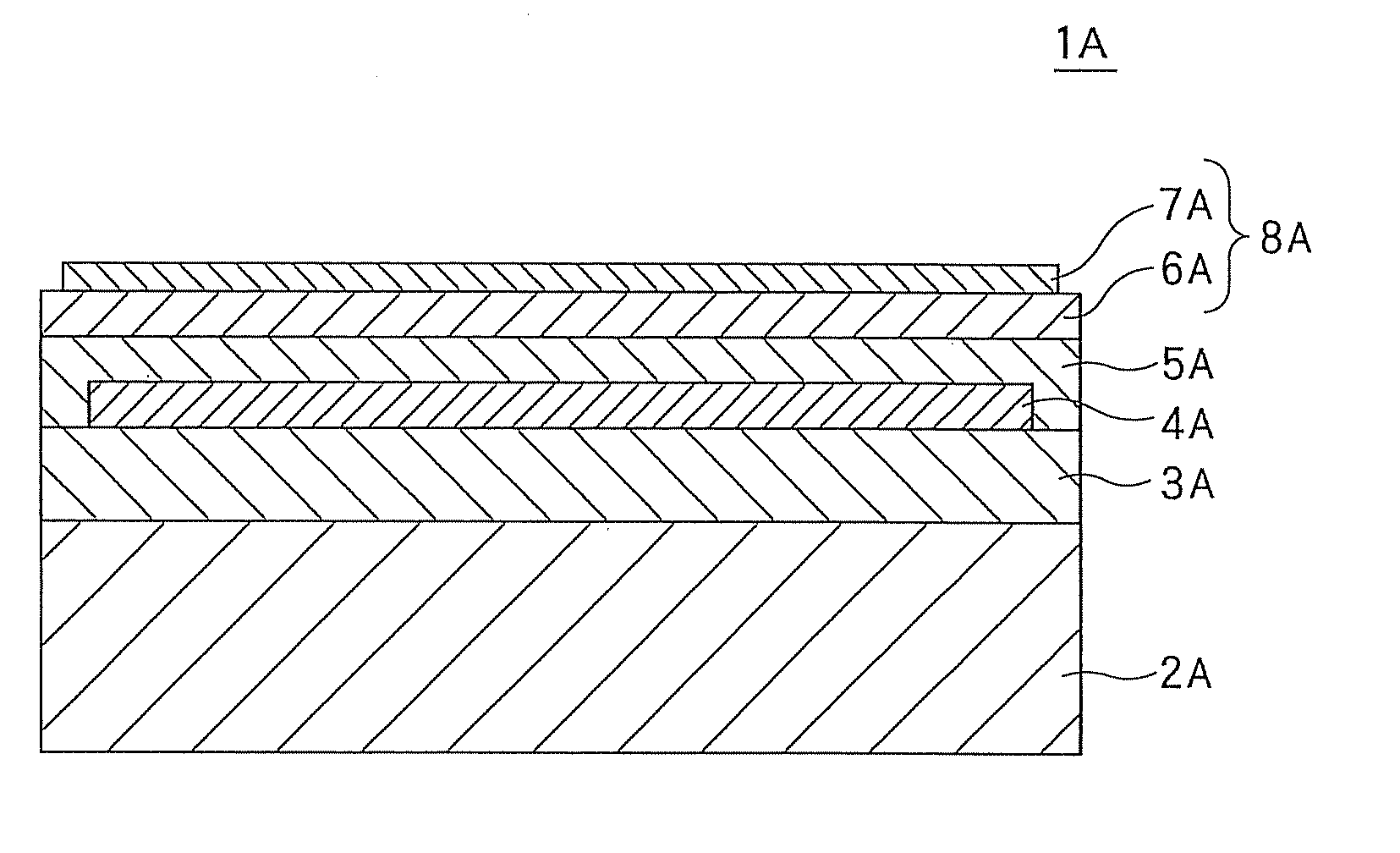
[0164]A 0.7 mm thick glass plate was used as a support. A photothermal conversion layer was formed on the support (photothermal conversion layer-forming step). More specifically, a resin precursor solution of a UV curable acrylic resin, containing a photopolymerization initiator and carbon blacks, was prepared, and the solution was applied onto the support by spin coating. Thereafter, the coating was irradiated with ultraviolet light to cure the resin, thereby forming a 1 μm thick photothermal conversion layer.

[0165]Next, a light blocking layer was formed on the photothermal conversion layer (light blocking layer-forming step). More specifically, aluminum was deposited onto the photothermal conversion layer by vacuum vapor deposition, thereby forming a 300 nm thick aluminum film as a light blocking layer. The light blocking layer was not formed on the entire surface of the photothermal conversion layer: the vacuum vapor deposition was carried out using a mask s...

example 2

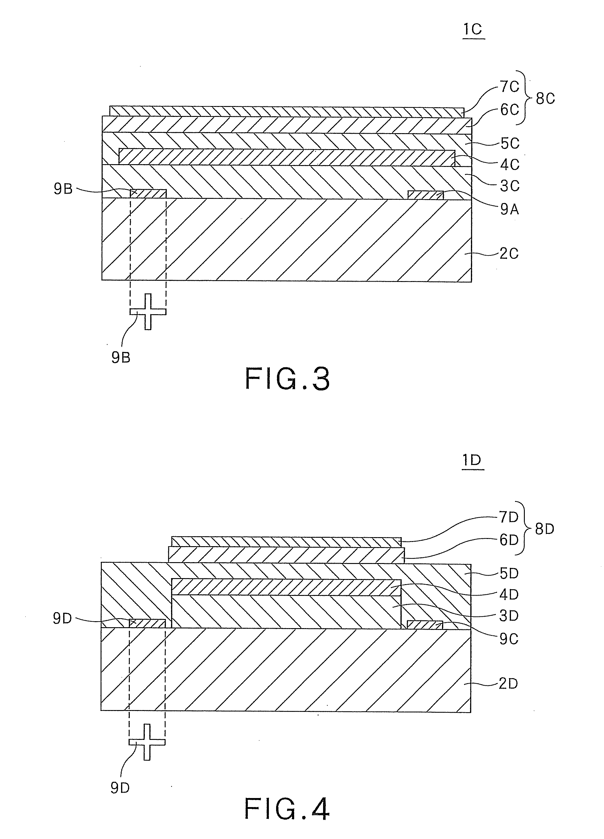
[0174]A laminate and a device were produced in the same manner as in Example 1 except that focus position-indicating marks were provided in the photothermal conversion layer. More specifically, as shown in the laminate 1D of FIG. 4, a region where the photothermal conversion layer 3D is not formed was provided, and focus position-indicating marks 9C, 9D, each having a cross shape, were formed at five positions on the support by vacuum vapor deposition of aluminum using a mask (focus position-indicating mark-forming step). In the photothermal conversion layer detachment step, the photothermal conversion layer was irradiated with YAG laser light after focusing the laser light on the focus position-indicating marks by using a laser emitting device.

[0175]For the organic EL device thus obtained, the light-emitting properties were evaluated in the same manner as in Example 1. As a result, the entire 1 mm×1 mm light-emitting area was found to be luminous. No damaged area was observed even ...


PUM

PropertyMeasurementUnit
strain pointaaaaaaaaaa
thicknessaaaaaaaaaa

Abstract

There are provided a laminate, a preparatory support, a laminate production method and a device production method which make it possible to successfully produce a thin device on a flexible substrate which is likely to bend or break. A laminate 1A includes: a support 2A; a photothermal conversion layer 3A; a light blocking layer 4A; an adhesive layer 5A; a flexible substrate 6A; and a device element 7A, wherein the support 2A can be detached from the other layers by irradiating the photothermal conversion layer 3A with light, and wherein the adhesive layer 5A is formed such that it covers the side surface of the light blocking layer 4A.

Description

CROSS-REFERENCE TO RELATED APPLICATIONS[0001]The present patent application benefits from Japanese Patent Application No. 2009-224790 filed on Sep. 29, 2009, the entire content of which is hereby incorporated by reference into the present application.BACKGROUND OF THE INVENTION[0002]1. Field of the Invention[0003]The present invention relates to a laminate, a preparatory support for producing the laminate, a method for producing a laminate, and a method for producing a device.[0004]2. Background Art[0005]In the field of semiconductor technology, studies are being made to produce a thinner semiconductor wafer (hereinafter also referred to simply as “wafer”) in order to respond to the progress toward thinner packages and higher-density devices through development of chip stacking techniques. Thinning of a wafer is performed by so-called back grinding, i.e. grinding of a wafer surface opposite to a patterned surface. Due to warpage of a wafer caused by thinning, however, such wafer thi...

Claims


Application Information

Patent Timeline
Patent Type & Authority Applications(United States)
IPC IPC(8): H01L51/05B32B7/06B32B17/06H01L51/40
CPCH01L51/003H01L51/0097Y10T428/24843H01L2251/5338Y02E10/549H01L51/56Y02P70/50H10K71/80H10K77/111H10K2102/311H10K71/00
Inventor KOBAYASHI, YOSHIHIROTAKEDA, TOSHIHIKO
Owner DAI NIPPON PRINTING CO LTD
Why Eureka
Try Eureka