Semiconductor memory device and a method of controlling a semiconductor memory device

a memory device and semiconductor technology, applied in the direction of information storage, static storage, instruments, etc., can solve the problems of long programming time, increased testing cost, and difficulty in precisely judging the program status of the anti-fuse element, so as to achieve the effect of reducing the processing tim

Active Publication Date: 2011-03-31
RENESAS ELECTRONICS CORP
View PDF2 Cites 7 Cited by
  • Summary
  • Abstract
  • Description
  • Claims
  • Application Information

AI Technical Summary

Benefits of technology

[0016]In contrast, according to the configuration of the present invention, the first-conductivity-type first region and the second region, respectively having the first anti-fuse element and the second anti-fuse element to be concomitantly programmed formed therein, are isolated by the second-conductivity-type third region having the different conductivity type. Accordingly, for example, even if the gate insulating film causes breakdown in the first anti-fuse element to produce hot carriers, and the holes are consequently injected from the first anti-fuse element to the first region, the second region may successfully be prevented from elevating in the potential. Also the first region may be prevented from elevating in the potential due to influences by the second anti-fuse elements. Accordingly, each anti-fuse element may keep a desirable level of difference of potential between the gate electrode and the substrate, without being affected by the other anti-fuse element, so that each anti-fuse element may be applied with a desired level of programming voltage, and thereby the plurality of anti-fuse elements may successfully be programmed at a time. As a consequence, a substantial time of programming and costs for testing may be reduced.
[0018]According to the present invention, a plurality of anti-fuse elements may be programmed at a time, and thereby the process time may be reduced.

Problems solved by technology

It has, however, been difficult to exactly judge a program status of the anti-fuse element, due to variation in the processes and variation in current after breakdown of the anti-fuse element.
The programming therefore takes a long time, and undesirably raises a cost for testing.
In this configuration, an effort of concomitantly breaking a plurality of anti-fuse elements may fail in applying a desired level of programming voltage to the selected cells, due to potential drop induced by program current.
For this reason, an attempt to induce breakdown in a plurality of anti-fuse elements at a time will result in a large increase in the substrate potential due to the holes injected into the substrate.
As a consequence, difference in potential between the gate electrodes and the substrate will be reduced in other anti-fuse elements not yet causing breakdown therein, enough to fail in applying a desired level of programming voltage, and thereby the breakdown may occasionally proceed unsuccessfully.
As described in the above, it has been difficult for the technique shown in FIG. 7 to concomitantly program a plurality of anti-fuse elements.
In this situation, increase in the number of memory cells to be concomitantly programmed may undesirably increase the substrate current.

Method used


Image

  • Semiconductor memory device and a method of controlling a semiconductor memory device
  • Semiconductor memory device and a method of controlling a semiconductor memory device
  • Semiconductor memory device and a method of controlling a semiconductor memory device

Examples


Embodiment Construction

[0027]The invention will now be described herein with reference to an illustrative embodiment. Those skilled in the art will recognize that many alternative embodiments can be accomplished using the teachings of the present invention and that the invention is not limited to the embodiments illustrated for explanatory purposes.

[0028]Embodiment of the present invention will be explained below, referring to the attached drawings. Note that all similar constituents in all drawings will be given similar reference numerals or symbols, and explanations therefor will not always be repeated.

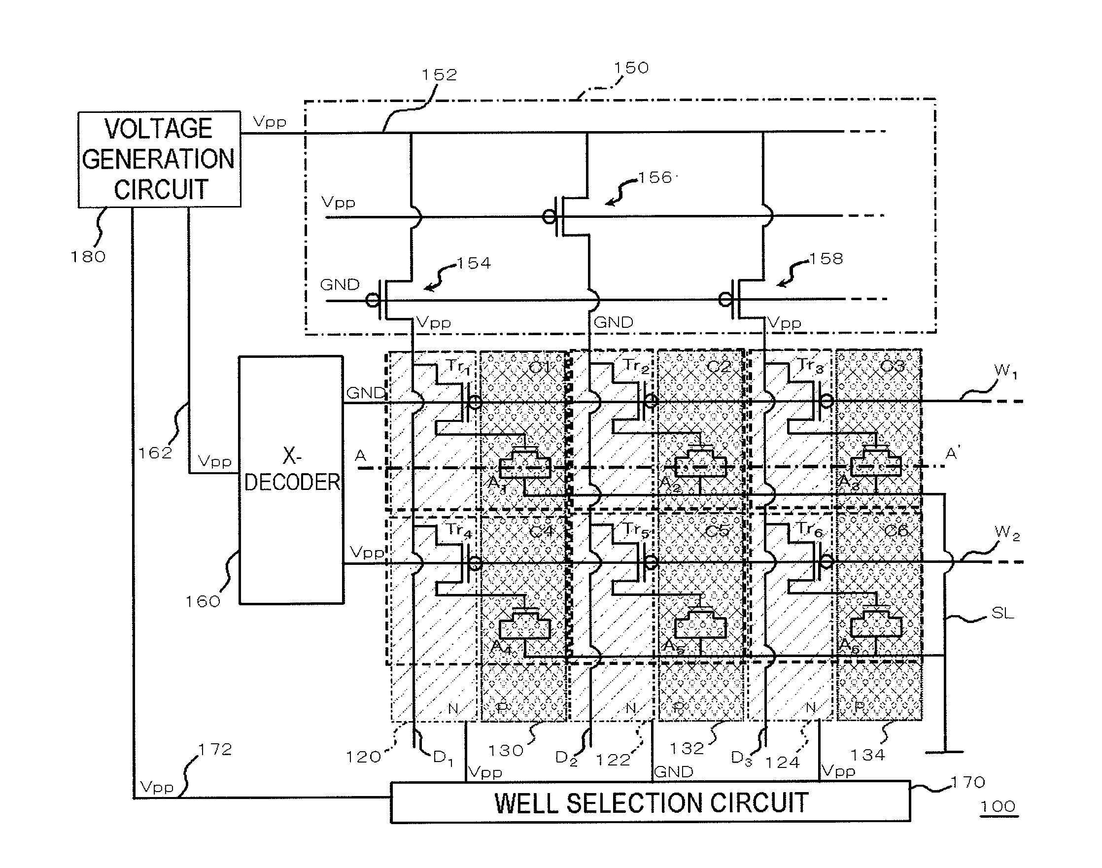
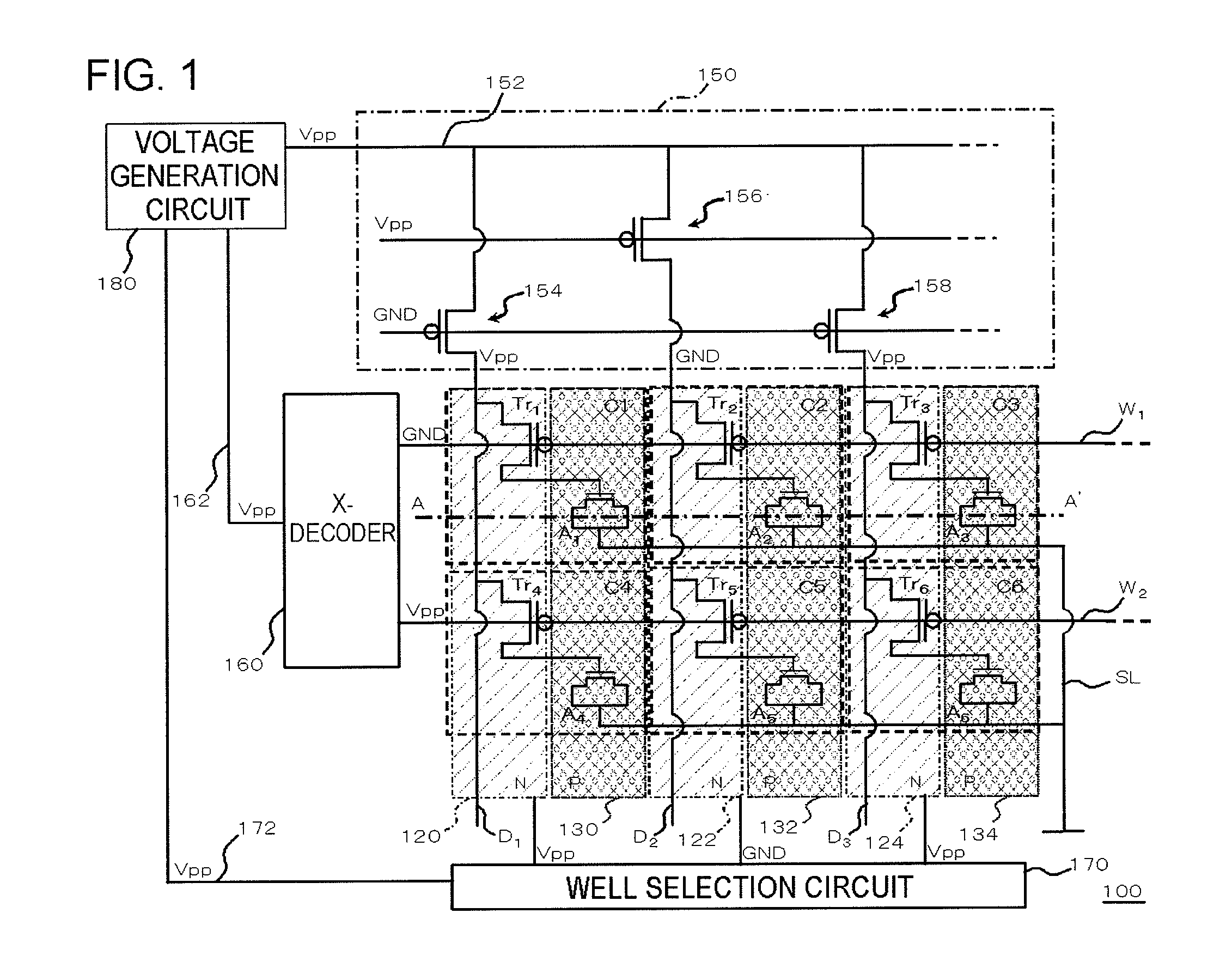
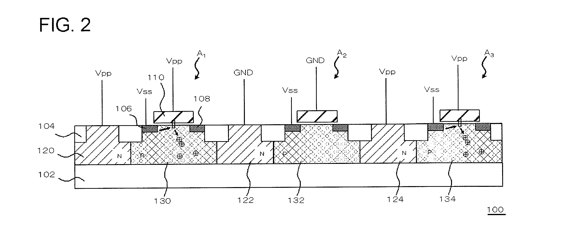
[0029]FIG. 1 is a circuit diagram illustrating an exemplary configuration of a semiconductor memory device of an embodiment of the present invention. FIG. 2 is a sectional view illustrating a layout which appears at a cross section taken along line A-A′ in FIG. 1. FIG. 1 and FIG. 2 illustrate a status of programming carried out by applying a predetermined level of programming voltage to the anti-fuse elem...


PUM


Abstract

A semiconductor memory device includes a first anti-fuse element and a second anti-fuse element, respectively composed of a transistor, wherein the first anti-fuse element and the second anti-fuse element are configured so as to be concomitantly programmable, respectively formed in P-wells on a substrate, and the adjacent P-wells are isolated by N-wells of an opposite conductivity type, formed therebetween.

Description

[0001]This application is based on Japanese patent application No. 2009-224896 the content of which is incorporated hereinto by reference.BACKGROUND[0002]1. Technical Field[0003]The present invention relates to a semiconductor memory device and a method of controlling a semiconductor memory device, and in particular to a semiconductor memory device which contains anti-fuse elements, and a method of controlling such semiconductor memory device.[0004]2. Background Art[0005]In these years, anti-fuse memory making use of anti-fuse elements typically composed of transistors and so forth has been known. Write-in operation (programming) into the anti-fuse memory is accomplished by causing breakdown of a gate insulating film in each anti-fuse element, to thereby electrically connect a gate electrode and an impurity-diffused region formed in a surficial portion of a substrate.[0006]It has, however, been difficult to exactly judge a program status of the anti-fuse element, due to variation in...

Claims


Application Information

Patent Timeline
Patent Type & Authority Applications(United States)
IPC IPC(8): G11C17/16
CPCG11C17/18G11C17/16
Inventor KODAMA, NORIAKIONUMA, TAKUJI
Owner RENESAS ELECTRONICS CORP
Why Eureka
Try Eureka