

MEMS microphone package
a microphone and microelectromechanical technology, applied in the field of microelectromechanicalsystems (mems) microphone packages, can solve the problem of more difficult to miniaturize the volume of the microphon
- Summary
- Abstract
- Description
- Claims
- Application Information
AI Technical Summary
Benefits of technology
Problems solved by technology
Method used
Image

Examples
first embodiment
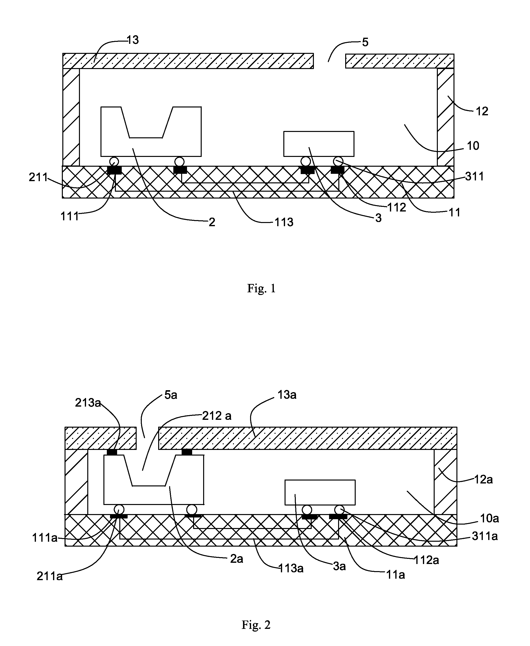
Referring to FIG. 1, a MEMS microphone package of the present invention is disclosed. The MEMS microphone package includes a base 11, a sidewall 12 extending from the base 11, and a cover 13 supported by the sidewall 12. The combination of the base 11, the sidewall 12 and the cover 13 forms a housing for providing a receiving space 10. The housing defines an acoustic hole 5 for receiving external sound waves into the receiving space 10. The MEMS microphone package further includes a MEMS die 2 and a chip 3, such as an ASIC (Application Specific Integrated Circuit) chip 3 accommodated in the receiving space 10. As shown in FIG. 1, the MEMS die 2 and the ASIC chip 3 are both mounted on the base 11. The MEMS die 2 defines a plurality of first conductive pads 211, and the ASIC chip 3 defines a plurality of second conductive pads 311. Corresponding to the first conductive pads 211 and the second conductive pads 311 respectively, the base 11 defines a plurality of first conductive areas 1...
second embodiment
Referring to FIG. 2, a MEMS microphone package of the present invention is disclosed. The MEMS microphone package includes a base 11a, a sidewall 12a extending from the base 11a, and a cover 13a supported by the sidewall 12a. The combination of the base 11a, the sidewall 12a and the cover 13a forms a housing for providing a receiving space 10a. The cover 13a defines an acoustic hole 5a for receiving external sound waves. The MEMS microphone package further includes a MEMS die 2a and an ASIC chip 3a accommodated in the receiving space 10a. As shown in FIG. 2, the MEMS die 2a and the ASIC chip 3a are both mounted on the base 11a. The MEMS die 2a defines a plurality of first conductive pads 211a, and the ASIC chip 3a defines a plurality of second conductive pads 311a. Corresponding to the first conductive pads 211a and the second conductive pads 311a respectively, the base 11a defines a plurality of first conductive areas 111a and a plurality of second conductive areas 112a. The MEMS d...
third embodiment
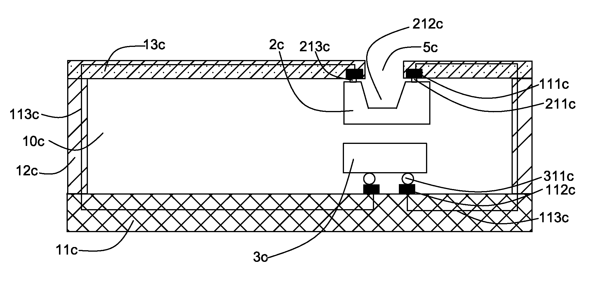
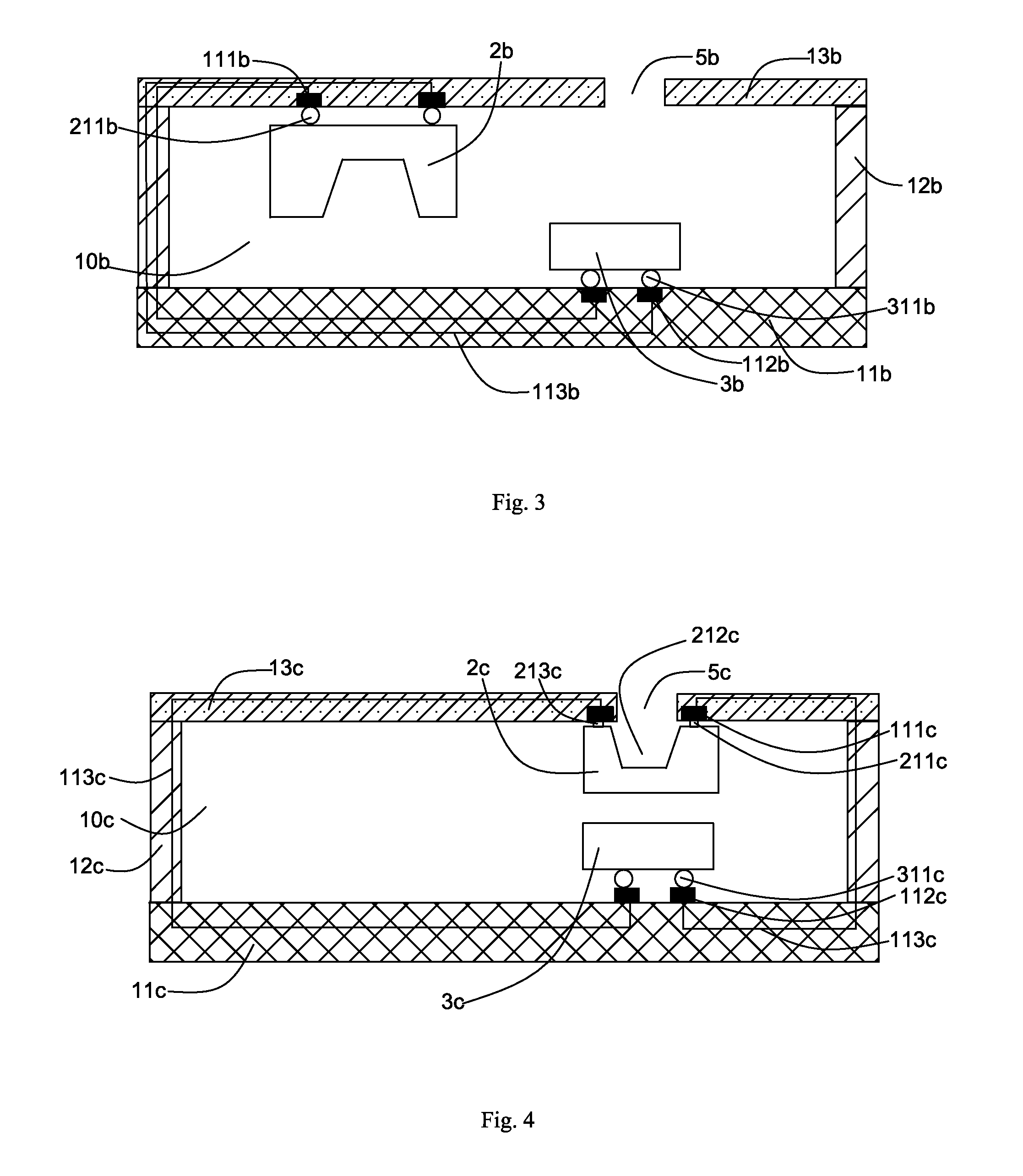
Referring to FIG. 3, a MEMS microphone package of the present invention is disclosed. The MEMS microphone package includes a base 11b, a sidewall 12b extending from the base 11b, and a cover 13b supported by the sidewall 12b. The combination of the base 11b, the sidewall 12b and the cover 13b forms a housing for providing a receiving space 10b. The cover 13b defines an acoustic hole 5b for receiving external sound waves into the receiving space 10b. The MEMS microphone package further includes a MEMS die 2b and an ASIC chip 3b accommodated in the receiving space 10b. As shown in FIG. 3, the MEMS die 2b is mounted on the cover and the ASIC chip 3b is mounted on the base 11b. The MEMS die 2b defines a plurality of first conductive pads 211b, and the ASIC chip 3b defines a plurality of second conductive pads 311b. Corresponding to the first conductive pads 211b, the cover 13b defines a plurality of first conductive areas 111b. Corresponding to the second conductive pads 311b, the base ...
PUM
 Abstract
Description
Claims
Application Information