CMOS compatible MEMS microphone and method for manufacturing the same

A microphone and backplane technology, applied in the field of microphones, can solve problems such as affecting device function and manufacturing yield, and difficult to control the intrinsic stress of CMOS thin films

Active Publication Date: 2012-12-12
GOERTEK MICROELECTRONICS CO LTD
View PDF10 Cites 53 Cited by
  • Summary
  • Abstract
  • Description
  • Claims
  • Application Information

AI Technical Summary

Problems solved by technology

However, it is difficult to control the intrinsic stress in CMOS films, which affects device functionality and fabrication yield

Method used


Image

  • CMOS compatible MEMS microphone and method for manufacturing the same
  • CMOS compatible MEMS microphone and method for manufacturing the same
  • CMOS compatible MEMS microphone and method for manufacturing the same

Examples


no. 1 example )

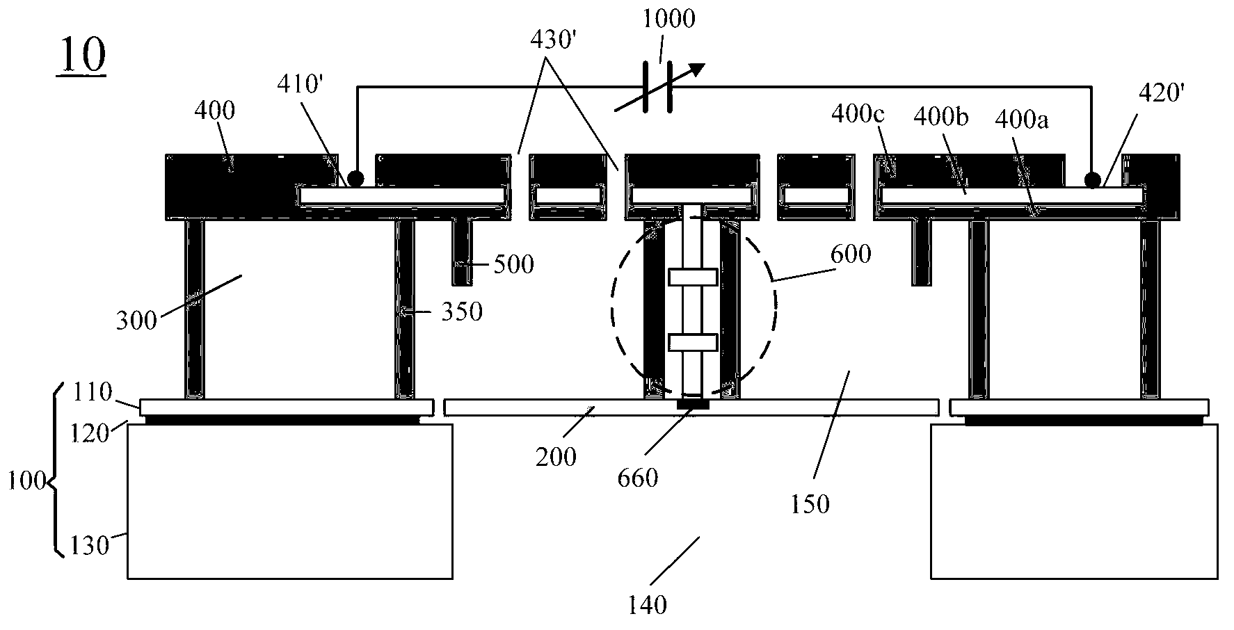
[0036] First, refer to figure 1 The specific structure of the CMOS-compatible MEMS microphone described in the first embodiment of the present invention will be described. figure 1 is a sectional view showing the structure of the CMOS-compatible MEMS microphone 10 according to the first embodiment of the present invention.

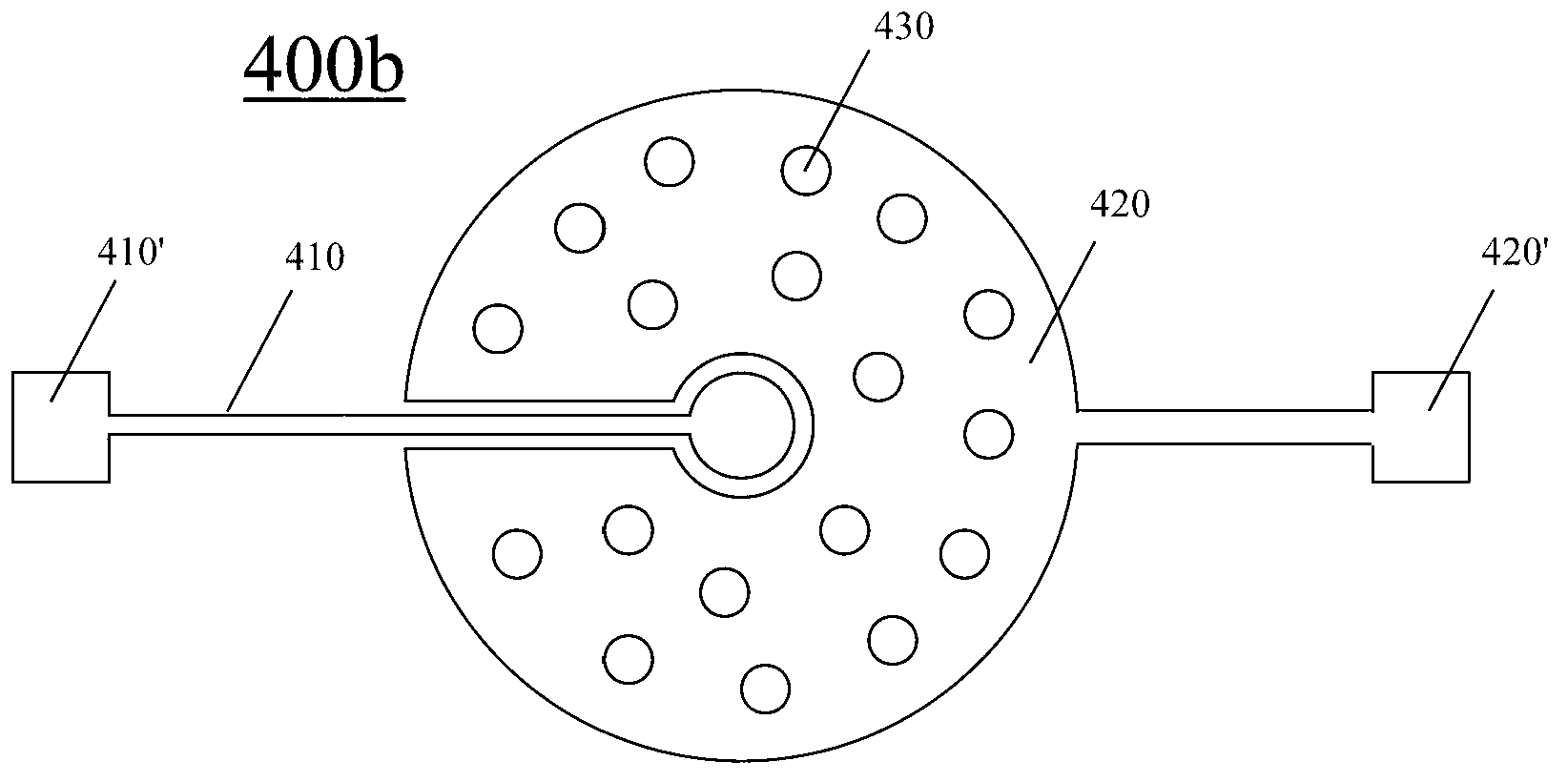
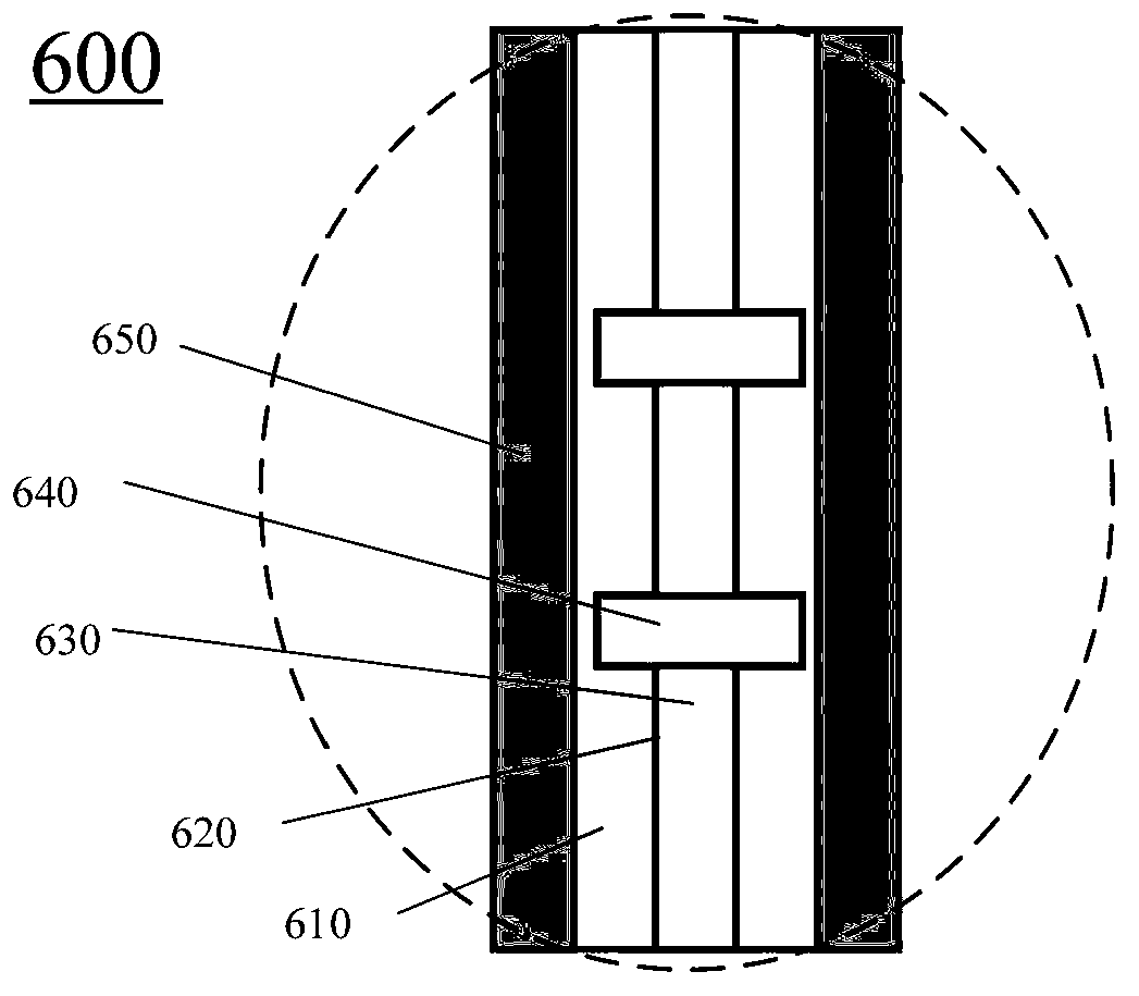
[0037] Such as figure 1 As shown, the CMOS-compatible MEMS microphone 10 includes: a silicon-on-insulator (SOI) substrate 100 , a microphone diaphragm 200 , an isolator 300 , a microphone backplate 400 , a plurality of dimples 500 and interconnection posts 600 .

[0038] The SOI substrate 100 includes a silicon device layer 110 , a buried oxide (BOX) layer 120 , and a silicon substrate 130 stacked from top to bottom in the following order. The SOI substrate 100 has openings in the silicon substrate 130 and the BOX layer 120 to expose the lower surface of the microphone diaphragm 200 , thus forming the back hole 140 .

[0039] Diaphragm 200 is formed fro...

no. 2 example )

[0059] The following will refer to Figure 5 The specific structure of the CMOS-compatible MEMS microphone described in the second embodiment of the present invention will be described. Figure 5 is a sectional view showing the structure of the CMOS-compatible MEMS microphone 10' according to the second embodiment of the present invention. Will Figure 5 and figure 1 In comparison, the difference between the second embodiment of the present invention and the first embodiment is that, in the second embodiment, the interconnection column 600' is designed to be arranged on the edge of the diaphragm 200.

[0060] Accordingly, in the second embodiment, the diaphragm 200 is not separated from the SOI substrate 100, that is, the edge portion of the diaphragm 200 is anchored. Therefore, preferably, the intrinsic stress of the prepared silicon device layer 110 of the SOI substrate 100 is small, so that the performance of the diaphragm 200 is less affected.

[0061] In addition, in ...


PUM


Abstract

The present invention relates to a CMOS compatible MEMS microphone, comprising: an SOI substrate, wherein a CMOS circuitry is accommodated on its silicon device layer; a microphone diaphragm formed with a part of the silicon device layer, wherein the microphone diaphragm is doped to become conductive; a microphone backplate including CMOS passivation layers with a metal layer sandwiched and a plurality of through holes, provided above the silicon device layer, wherein the plurality of through holes are formed in the portions thereof opposite to the microphone diaphragm, and the metal layer forms an electrode plate of the backplate; a plurality of dimples protruding from the lower surface of the microphone backplate opposite to the diaphragm; and an air gap, provided between the diaphragm and the microphone backplate, wherein a spacer forming a boundary of the air gap is provided outside of the diaphragm or on the edge of the diaphragm; wherein a back hole is formed to be open in substrate underneath the diaphragm so as to allow sound pass through, and the microphone diaphragm is used as an electrode plate to form a variable capacitive sensing element with the electrode plate of the microphone backplate.

Description

technical field [0001] The invention relates to the technical field of microphones, in particular to a CMOS-compatible MEMS microphone and a manufacturing method thereof. Background technique [0002] Silicon-based MEMS microphones, also known as acoustic transducers, have been in development for many years. Silicon-based MEMS microphones can be widely used in many applications such as mobile phones, hearing aids, smart toys, and surveillance devices due to their potential advantages in miniaturization, performance, reliability, environmental durability, cost, and mass production capability. [0003] Generally speaking, a silicon-based MEMS microphone consists of four components: a fixed backplate, a highly compliant movable diaphragm (which together form the two plates of a variable air-gap capacitor), a voltage bias source, and a buffer. The two mechanical elements, the backplate and the diaphragm, are usually formed on a single silicon substrate. One of these two elemen...

Claims


Application Information

Patent Timeline
Patent Type & Authority Applications(China)
IPC IPC(8): B81B7/00B81C1/00H04R7/00
CPCB81C1/00246B81C2203/0714B81C2203/0735B81B2201/0221B81B2207/015H04R19/04H04R19/005B81B2201/0257H04R31/00
Inventor 王喆
Owner GOERTEK MICROELECTRONICS CO LTD
Why Eureka
Try Eureka