Method for Calculating Capacitance Gradients in VLSI Layouts Using A Shape Processing Engine

Inactive Publication Date: 2011-03-31
GLOBALFOUNDRIES INC
View PDF5 Cites 20 Cited by
  • Summary
  • Abstract
  • Description
  • Claims
  • Application Information

AI Technical Summary

Benefits of technology

[0012]In another aspect of the invention, a method and a system are provided for determining capacitance gradients of an integrated circuit chip layout in order to achieve a better performance. The method includes: a) decomposing one or more layout shapes into elementary patterns; b) translating physical parameter variations into variations on parameters of ele

Problems solved by technology

Needless to say, parasitic capacitances associated with interconnect materials within a VLSI circuit can result in unacceptable circuit performances.
However the constant increase in the number of process parameters impacting the shapes of a VLSI layout makes such an approach a methodology bottleneck and a more efficient approach for dealing with variations is needed.
As described above, the prior art does not address the problem of includin

Method used


Image

  • Method for Calculating Capacitance Gradients in VLSI Layouts Using A Shape Processing Engine
  • Method for Calculating Capacitance Gradients in VLSI Layouts Using A Shape Processing Engine
  • Method for Calculating Capacitance Gradients in VLSI Layouts Using A Shape Processing Engine

Examples


Example

[0035]The present invention and the various features and advantageous details thereof are explained more fully with reference to the non-limiting embodiments that are illustrated in the accompanying drawings and detailed in the following description of an embodiment of the invention.

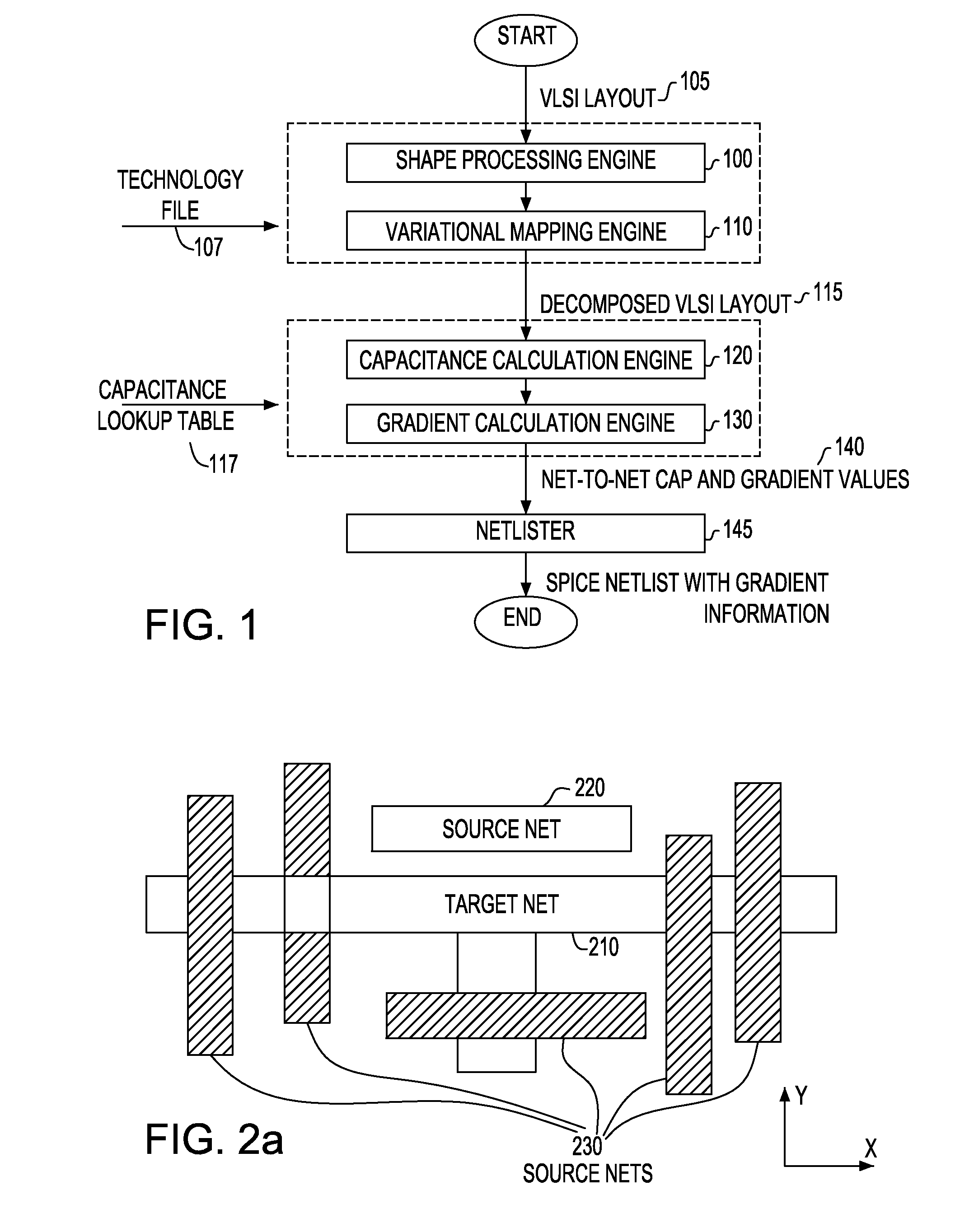
[0036]Referring to FIG. 1, there is shown a flowchart of a preferred embodiment of the invention that corrects the shortcomings found in the prior art and incorporates the calculation of gradients for capacitances based on the shape processing of a VLSI layout.

[0037]The flowchart shown in FIG. 1 further illustrates an embodiment of the invention showing a shape processing engine 100 feeding a variational map engine 110 whose role is to reflect variations in the shapes of the original VLSI layout. The input to the system and method is a VLSI layout file 105 describing the shapes of all the devices and wires connecting them on the integrated circuit (IC). These layout files can advantageously make use of i...


PUM


Abstract

Computing the gradients of capacitances in an integrated circuit chip layout with respect to design and process parameters is described. Included is a shape processing engine in the form of a variational mapping engine and a capacitance calculation engine that includes a gradient calculation engine. The variational mapping engine translates physical parameter variations into variations on the edges of the elementary patterns to which the layout of the integrated circuit is decomposed. The gradient calculation engine computes capacitance gradients by combining information from two sources. The first source consists of pre-existing gradients in a capacitance lookup table. The second source consists of analytical expressions of capacitance correction factors.

Description

TECHNICAL FIELD[0001]The present invention relates generally to the field of design automation of Very Large Scale Integrated circuit chips, and more particularly, to a system and method for extracting data for estimating the capacitance and for verifying and extracting electrical parameters based on geometric layouts.DESCRIPTION OF THE PRIOR ART[0002]During the course of designing a Very Large Scale Integrated (VLSI) circuit, it is desirable to render some form of circuit characterization in order to determine the performance of the circuit. The characteristic of a VLSI circuit is generally dependent upon two major factors, namely, parasitic capacitance and parasitic resistance. Needless to say, parasitic capacitances associated with interconnect materials within a VLSI circuit can result in unacceptable circuit performances. Hence, it is very important to calculate all the parasitic capacitances within a VLSI circuit in order to determine whether or not they exceed certain design ...

Claims


Application Information

Patent Timeline
IPC IPC(8): G06F17/50
CPCG06F17/5036G06F30/367
Inventor ELFADEL, IBRAHIM M.DEWEY, III, LEWIS WILLIAMEL-MOSELHY, TAREK A.WIDIGER, DAVID J.WILLIAMS, PATRICK M.
Owner GLOBALFOUNDRIES INC
Why Eureka
Try Eureka