This helps you quickly interpret patents by identifying the three key elements:
Problems solved by technology
Method used
Benefits of technology
[0027]According to the invention, a light emitting element that is capable of enhancing a light emission output in accordance with
Problems solved by technology
However, although the light emitting element disclosed in the JP-A-5-37017 is capable of broadening reflection wavelength region in a single body of the light reflection layer, if the light reflection layer has a thickness of not less than a predetermined value, the light emission output can not be increased, similarly to a case of usin
Method used
Image
Click on the blue label to locate the original text in one second.
Reading with bidirectional positioning of images and text.
Examples
first embodiment
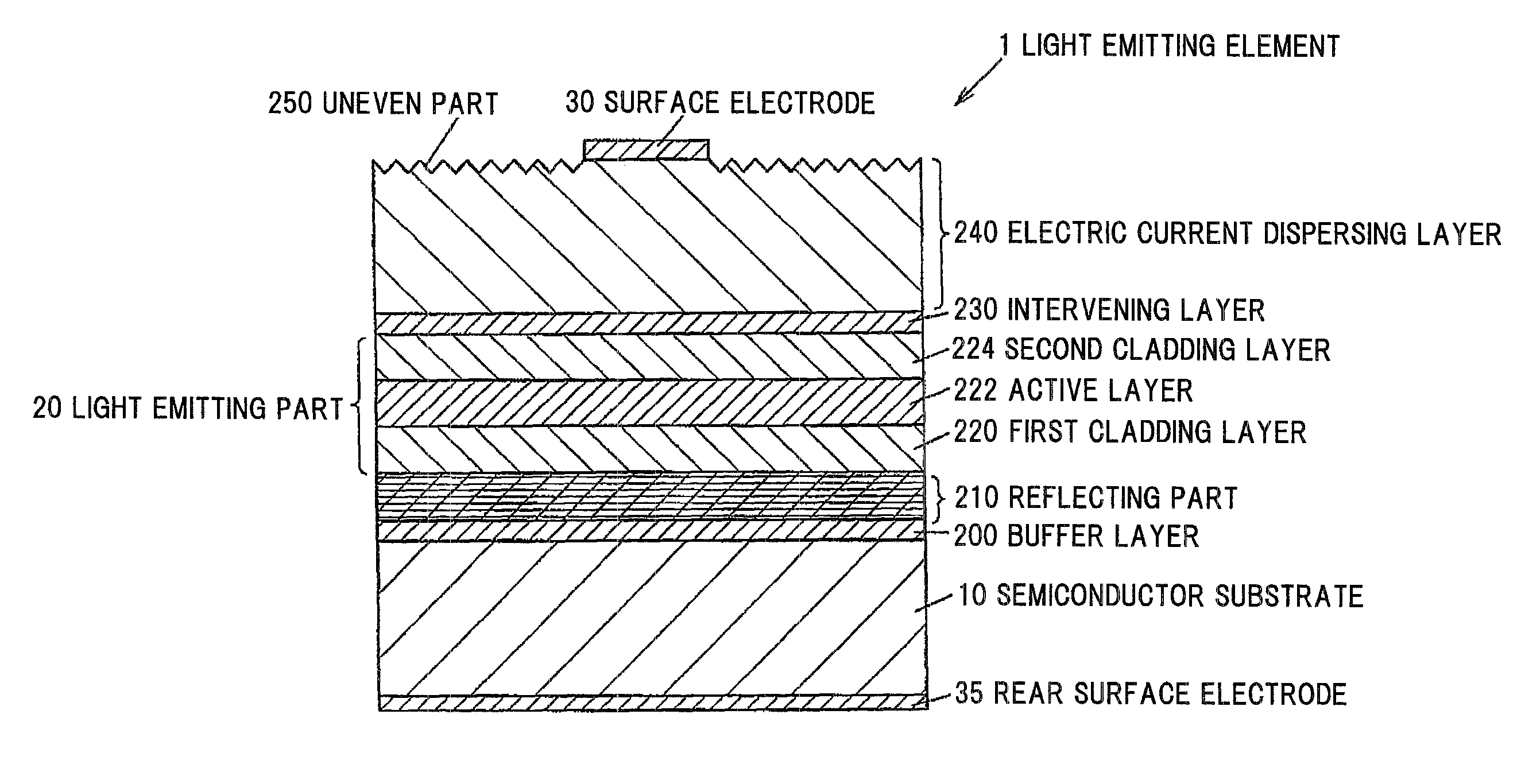
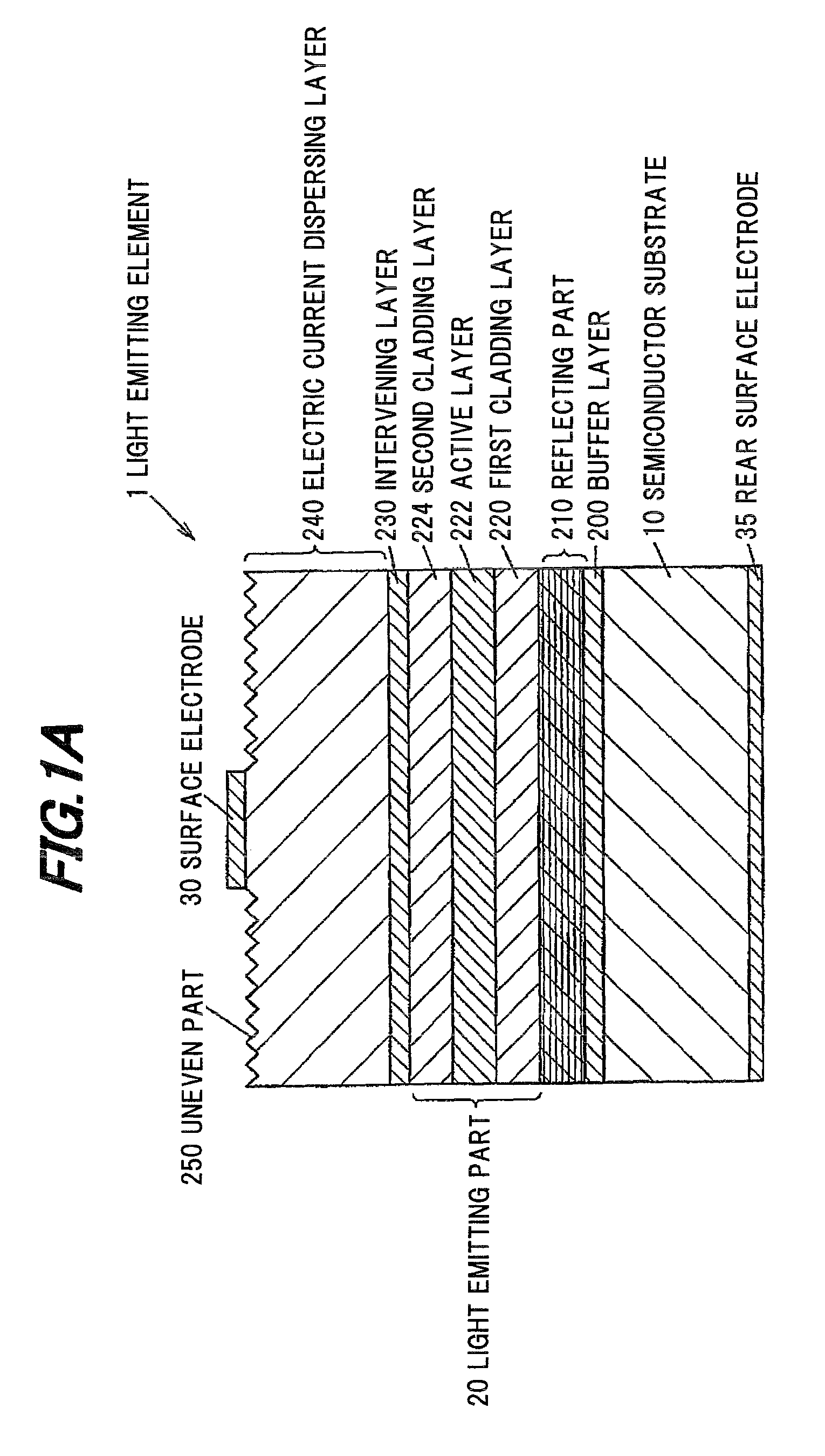
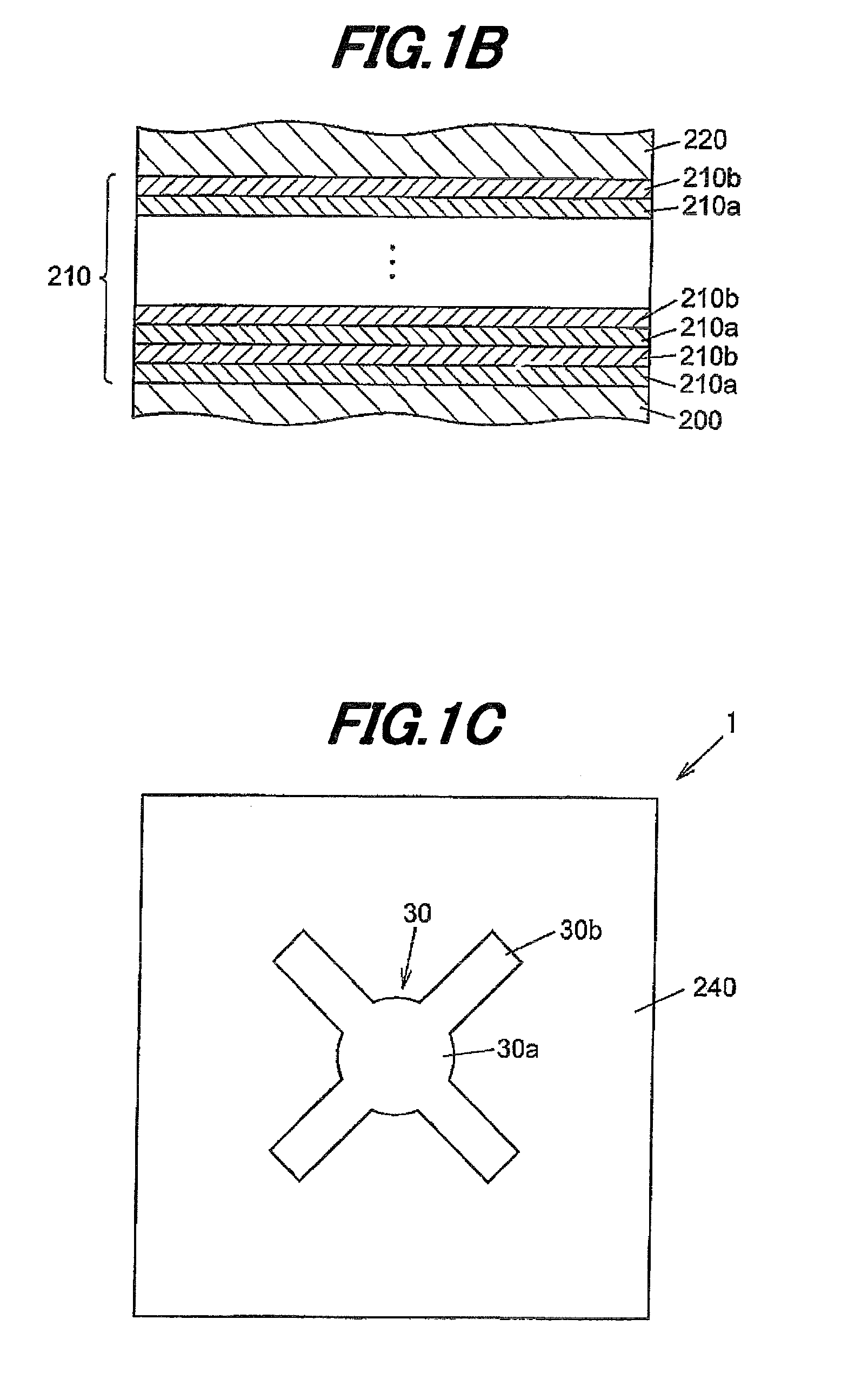
[0046]FIG. 1A is a cross-sectional view schematically showing a light emitting element according to a first embodiment of the invention, and FIG. 1B is a cross-sectional view schematically showing a reflecting part included in the light emitting element according to the first embodiment of the invention. Further, FIG. 1C is a plan view schematically showing a light emitting element according to a first embodiment of the invention.
[0047]Structural Outline of Light Emitting Element 1
[0048]The light emitting element 1 is, as an example, a light emitting diode (LED) for emitting a red light having peak wavelength (λP) adjacent to 631 nm. Particularly, the light emitting element 1 includes an n-type as a first conductivity type semiconductor substrate 10, an n-type buffer layer 200 disposed on the semiconductor substrate 10, a reflecting part 210 disposed on the buffer layer 200 so as to have a laminated structure of an n-type compound semiconductor, an n-type first cladding layer 220 di...
second embodiment
[0089]FIG. 2 is a cross-sectional view schematically showing a light emitting element according to a second embodiment of the invention.
[0090]The light emitting element 1a according to the second embodiment includes almost the same composition as the light emitting element 1 according to the first embodiment except for further including a light extracting layer 40 on the uneven part 250, difference from the light emitting element 1 according to the first embodiment. Therefore, detail explanation will be omitted except for the different points.
[0091]The light emitting element 1a includes the light extracting layer 40 formed on the surface of the electric current dispersing layer 240 except for a region where the surface electrode 30 is formed so as to be formed of a material being transparent to the light emitted from the active layer 222 and having refractive index at the level intermediate between the semiconductor constituting the electric current dispersing layer 240 and air. The...
third embodiment
[0094]FIG. 3 is a cross-sectional view schematically showing a light emitting element according to a third embodiment of the invention.
[0095]The light emitting element 1b according to the third embodiment includes almost the same composition as the light emitting element 1 according to the first embodiment except that the active layer 222 is sandwiched between a first undoped layer 221 and a second undoped layer 223, difference from the light emitting element 1 according to the first embodiment. Therefore, detail explanation will be omitted except for the different points.
[0096]Particularly, the light emitting element 1b according to the third embodiment includes the semiconductor substrate 10, the buffer layer 200 disposed on the semiconductor substrate 10, the reflecting part 210 disposed on the buffer layer 200, a first cladding layer 220 disposed on the reflecting part 210, the first undoped layer 221 disposed on the first cladding layer 220, the active layer 222 disposed on the...
PUM
Abstract
A light emitting element according to an embodiment of the invention includes a semiconductor substrate, a light emitting part having a first conductivity type first cladding layer; a second conductivity type second cladding layer different from the first cladding layer in the conductivity type and an active layer sandwiched between the first cladding layer and the second cladding layer, a reflecting part for reflecting a light emitted from the active layer, disposed between the semiconductor substrate and the light emitting part so as to have a thickness of 1.7 μm to 8.0 μm and an electric current dispersing layer disposed on a side of the light emitting part opposite to the reflecting part, having a uneven part on the surface thereof, wherein the reflecting part is formed so as to have at least three pair layers formed of a first semiconductor layer and a second semiconductor layer different from the first semiconductor layer, the first semiconductor layer has a thickness TA defined by the formula (1), if peak wavelength of the light emitted from the active layer is λP, refractive index of the first semiconductor layer is nA, refractive index of the second semiconductor layer is nB, refractive index of the first cladding layer is nIn, and incident angle of light to the second semiconductor layer is θ, the second semiconductor layer has a thickness TB defined by the formula (2), and a plurality of pair layers of the reflecting part have a different thickness to each other according as values of the incident angle of light θ in the formulae (1) and (2) are different with respect to each pair layer, and at least one pair layer includes the first semiconductor layer and the second semiconductor layer defined by that the incident angle of light θ is not less than 50 degrees.
Description
[0001]The present application is based on Japanese patent application No. 2009-231157 filed on Oct. 5, 2009, the entire contents of which are incorporated herein by reference.BACKGROUND OF THE INVENTION[0002]1. Field of the Invention[0003]This invention relates to a light emitting element. In particular, this invention relates to a light emitting element including a semiconductor substrate opaque to a light emitted from an active layer and a reflecting part disposed between the semiconductor substrate and the active layer so as to have a thickness of not less than a predetermined value.[0004]2. Description of the Related Art[0005]Conventionally, a light emitting element is known that includes an n-type GaAs substrate, a light reflection layer disposed on the n-type GaAs substrate, an n-type Al0.45Ga0.55As cladding layer disposed on the light reflection layer, a p-type GaAs active layer disposed on the n-type Al0.45Ga0.55As cladding layer, a p-type Al0.45Ga0.55As cladding layer dispo...
Claims
Application Information
Patent Timeline
Application Date:The date an application was filed.
Publication Date:The date a patent or application was officially published.
First Publication Date:The earliest publication date of a patent with the same application number.
Issue Date:Publication date of the patent grant document.
PCT Entry Date:The Entry date of PCT National Phase.
Estimated Expiry Date:The statutory expiry date of a patent right according to the Patent Law, and it is the longest term of protection that the patent right can achieve without the termination of the patent right due to other reasons(Term extension factor has been taken into account ).
Invalid Date:Actual expiry date is based on effective date or publication date of legal transaction data of invalid patent.