Light-emitting diode and method for manufacturing the same

a technology of light-emitting diodes and manufacturing methods, which is applied in the direction of semiconductor devices, semiconductor/solid-state device details, electrical apparatus, etc., can solve the problems of increasing manufacturing costs, and achieve the effects of reducing manufacturing costs, enhancing process yield, and reducing volume of the package structure of light-emitting diodes

Inactive Publication Date: 2011-04-07
CHI MEI LIGHTING TECH
View PDF39 Cites 22 Cited by
  • Summary
  • Abstract
  • Description
  • Claims
  • Application Information

AI Technical Summary

Benefits of technology

[0005]Therefore, one aspect of the present teachings is to provide a light-emitting diode and a method for manufacturing the same, in which a growth substrate may be used to replace a package frame, so that the volume of a packaged structure of the light-emitting diode can be reduced and the manufacturing cost can be decreased.
[0006]Another aspect of the present teachings is to provide a light-emitting diode and a method for manufacturing the same, in which the conduction locations of two electrodes of the light-emitting diode with horizontal electrodes type can be adjusted to the same side of a package structure, so that a wire bonding step can be omitted, and the light-emitting diode can be directly disposed on a circuit board. Therefore, the light-extracting area of the light-emitting diode device can be increased, and the problem of poor yield of wire bonding in the conventional design can be avoided.
[0007]Still another aspect of the present teachings is to provide a light-emitting diode and a method for manufacturing the same, which can use a substrate replacement technique to enhance the heat-dissipating efficiency, so that the life and the stability of the photoelectric quality of the light-emitting diode can be increased.
[0014]According to the aforementioned embodiments, by applying the present disclosure, the volume of the package structure of the light-emitting diode can be decreased, the manufacturing cost can be decreased, the light-extracting area of the light-emitting diode device can be increased, the process yield can be enhanced, and the life and the stability of the photoelectric quality of the light-emitting diode can be increased.

Problems solved by technology

However, in order to achieve this with a conventional packaging process, the volume of the packaged structure must be greatly increased which, in turn, increases the manufacturing cost.

Method used


Image

  • Light-emitting diode and method for manufacturing the same
  • Light-emitting diode and method for manufacturing the same
  • Light-emitting diode and method for manufacturing the same

Examples


Embodiment Construction

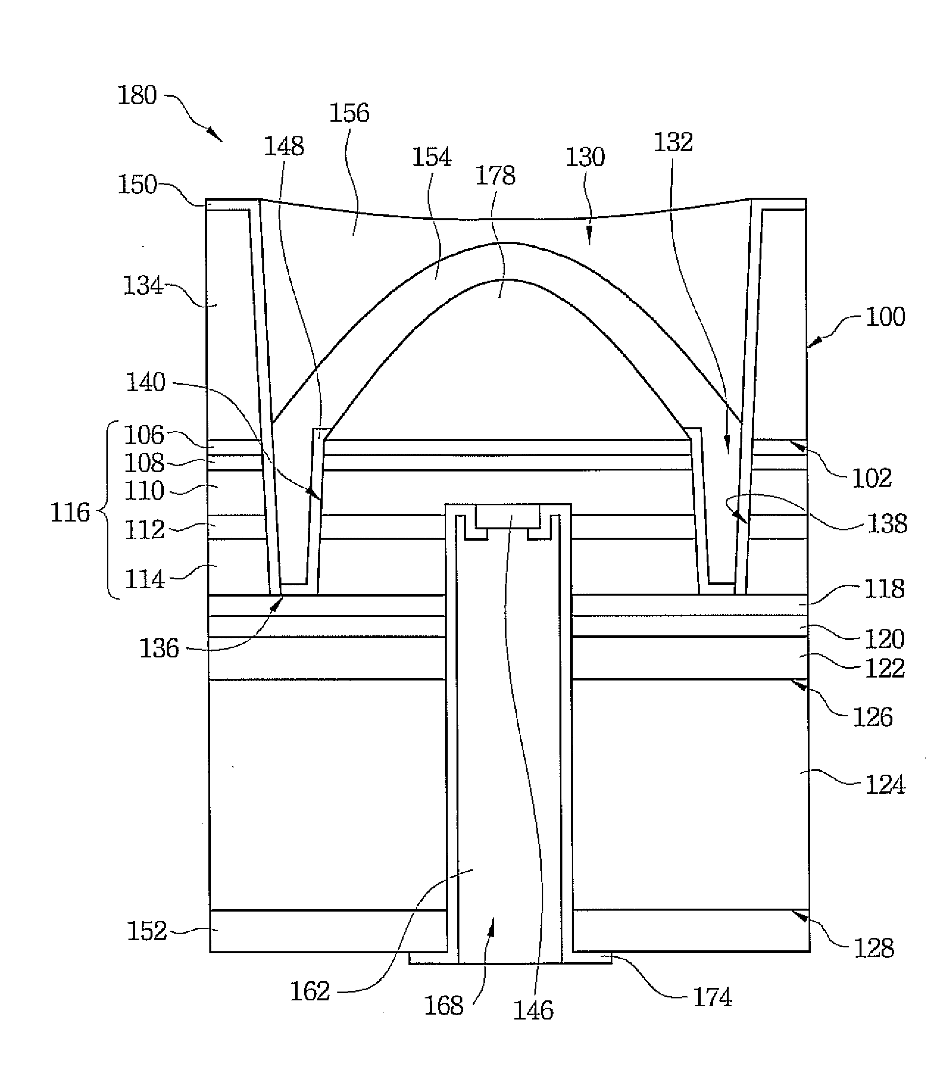
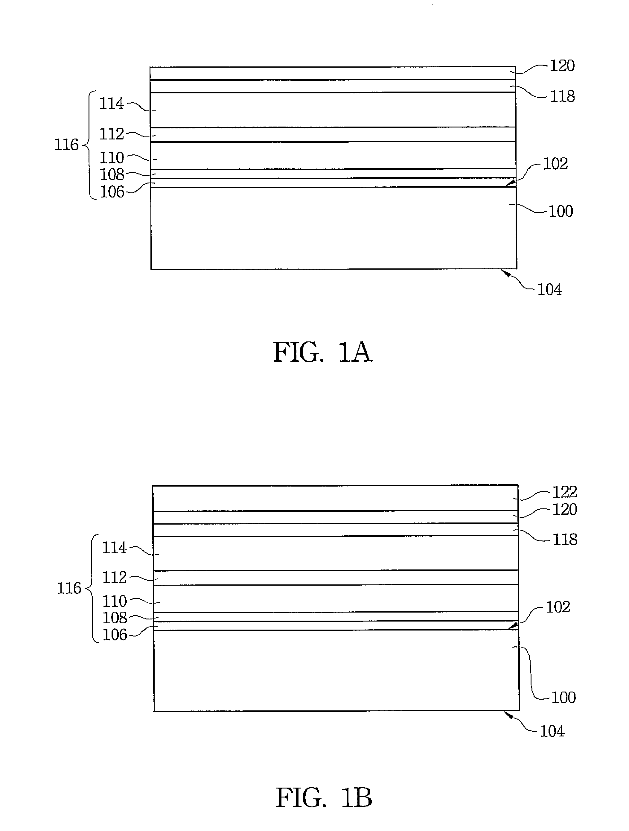
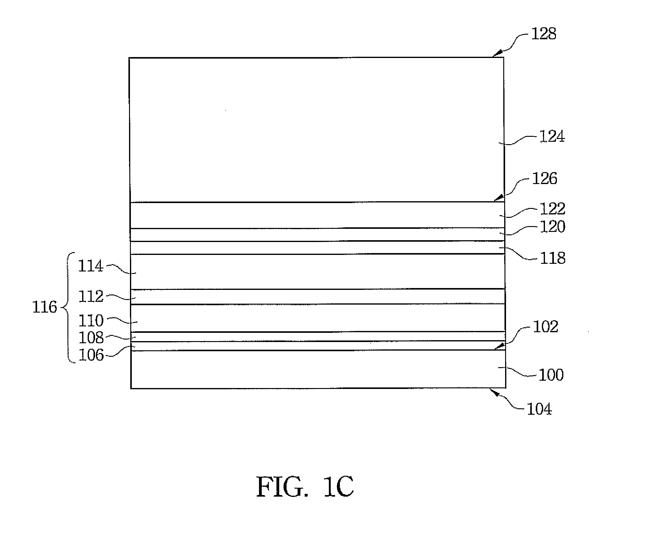
[0019]FIGS. 1A through 1F are schematic flow diagrams showing an exemplary process for manufacturing a light-emitting diode in accordance with an embodiment of the present teachings. In the present embodiment for manufacturing a light-emitting diode, a growth substrate 100 is firstly provided. The growth substrate 100 includes surfaces 102 and 104 on opposite sides. The material of the growth substrate 100 may include, but is not limited to, Al2O3, SIC or GaAs.

[0020]Then, an epitaxial structure 116 is formed on the surface 102 of the growth substrate 100 by, for example, an epitaxial growth method. In one embodiment, the epitaxial structure 116 may include a second conductivity type semiconductor layer 110, an active layer 112 and a first conductivity type semiconductor layer 114 stacked on the surface 102 of the growth substrate 100 in sequence. The first conductivity type semiconductor layer 114 and the second conductivity type semiconductor layer 110 have different conductivity t...


PUM

PropertyMeasurementUnit
depthaaaaaaaaaa
depthaaaaaaaaaa
thicknessaaaaaaaaaa

Abstract

A light-emitting diode and a method for manufacturing the same are described. The light-emitting diode includes a bonding substrate, a first conductivity type electrode, a bonding layer, an epitaxial structure, a second conductivity type electrode, a growth substrate and an encapsulant layer. The first conductivity type electrode and the bonding layer are respectively disposed on two surfaces of the bonding substrate. The epitaxial structure includes a first conductivity type semiconductor layer, an active layer and a second conductivity type semiconductor layer. A trench is set around the epitaxial structure and extends from the second conductivity type semiconductor layer to the first conductivity type semiconductor layer. The second conductivity type electrode is electrically connected to the second conductivity type semiconductor layer. The growth substrate is disposed on the epitaxial structure and includes a cavity exposing the epitaxial structure and the trench. The encapsulant layer is filled in the cavity.

Description

RELATED APPLICATIONS[0001]This application claims priority from Taiwan Patent Application Ser. No. 098133600, filed on Oct. 02, 2009, which is hereby incorporated by reference in its entirety.FIELD OF THE INVENTION[0002]The invention relates generally to a light-emitting device and, more particularly, to a light-emitting diode and a method for manufacturing the same.BACKGROUND OF THE INVENTION[0003]Currently, a conventional packaging process for a light-emitting diode mounts a light-emitting diode chip onto a package frame that can provide a protection function, and forms an encapsulant layer to cover and protect the light-emitting diode chip. Other than providing the light-emitting diode chip with a superior protection, the package frame also has to transmit electrical signals from an external circuit to the light-emitting diode chip for the operation of the light-emitting diode chip.[0004]However, in order to achieve this with a conventional packaging process, the volume of the pa...

Claims


Application Information

Patent Timeline
Patent Type & Authority Applications(United States)
IPC IPC(8): H01L33/00
CPCH01L33/20H01L33/54H01L33/382
Inventor YU, KUOHUIWANG, CHIENCHUNCHU, CHANGHSINLI, MENGHSIN
Owner CHI MEI LIGHTING TECH
Why Eureka
Try Eureka