
Mounting circuit substrate

Active Publication Date: 2011-04-07
MITSUBISHI ELECTRIC CORP
View PDF7 Cites 3 Cited by
  • Summary
  • Abstract
  • Description
  • Claims
  • Application Information

AI Technical Summary

Benefits of technology

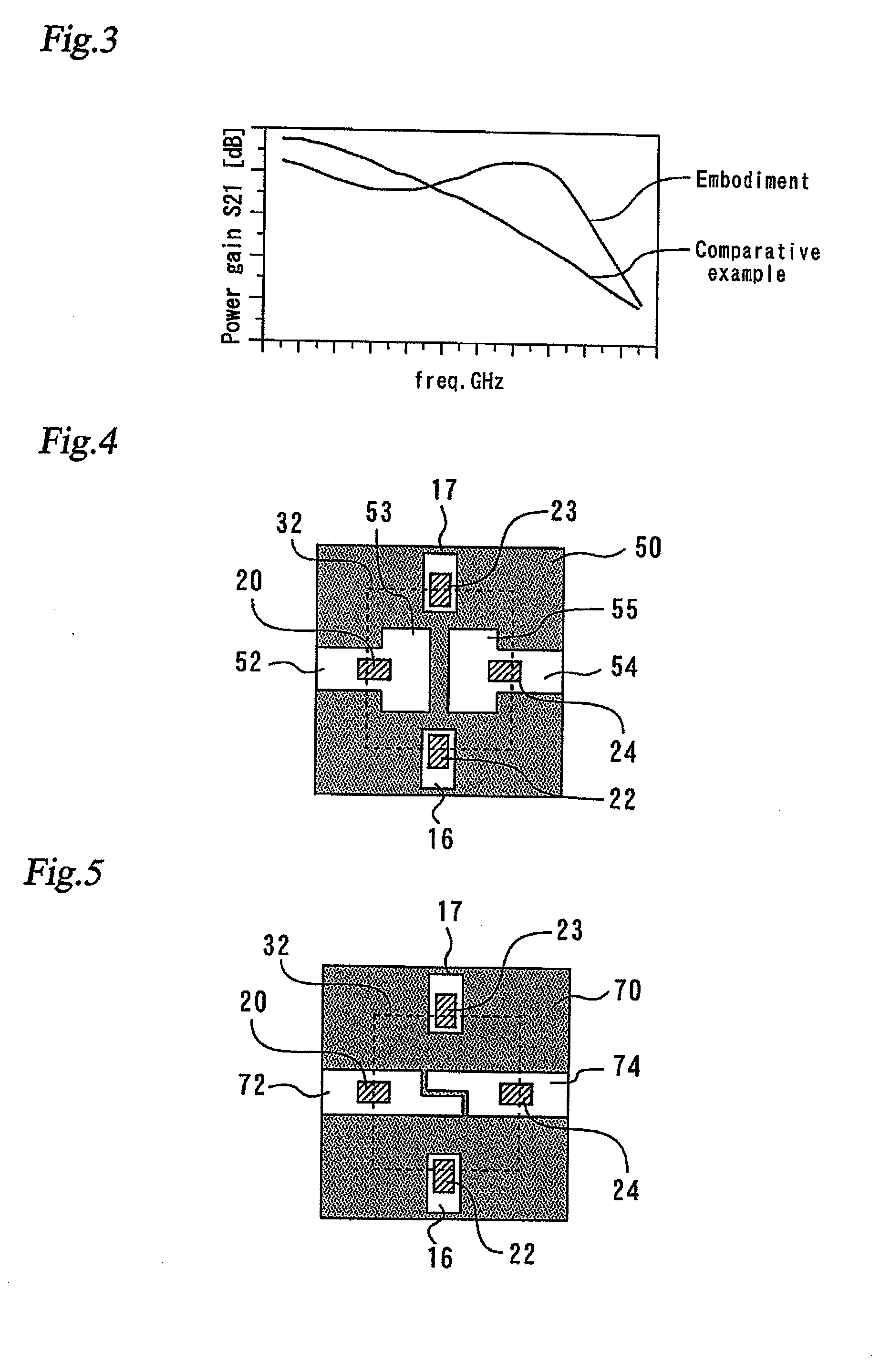
[0012]Thus, the mounting circuit substrate of the present invention is configured such that the capacitance between the gate and drain wiring conductors resonates with the LC components in the high frequency semiconductor device mounted on the substrate, thereby improving the power gain of the device.

Problems solved by technology

In high frequency applications, the electrical characteristics of the semiconductor devices are significantly affected by their operating frequency, which may cause various problems.
A problem associated with high frequency semiconductor devices is that the power gain decreases as the operating frequency increases.

Method used


Image

  • Mounting circuit substrate
  • Mounting circuit substrate
  • Mounting circuit substrate

Examples


first embodiment

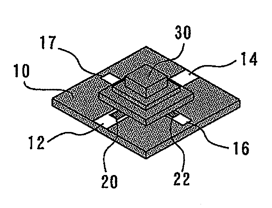
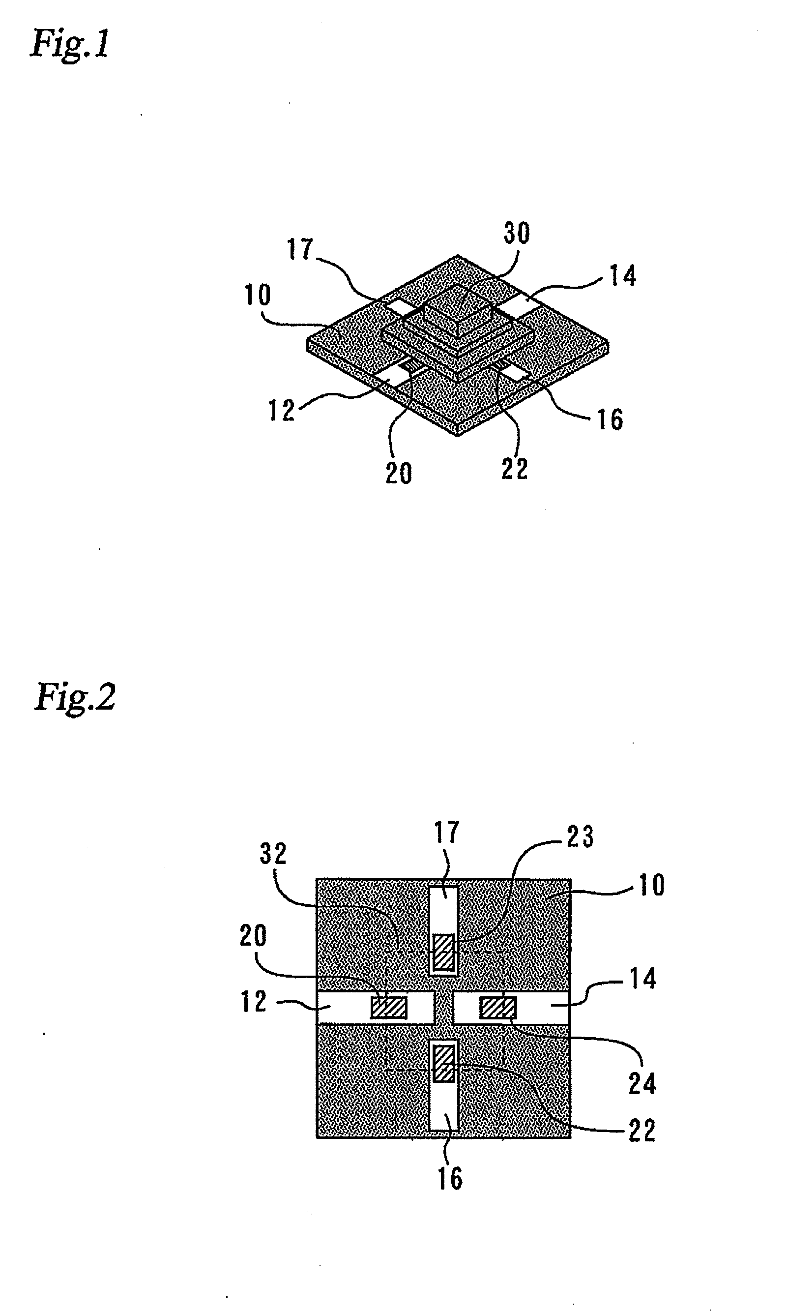
[0022]FIG. 1 is a perspective view of a mounting circuit substrate 10 according to a first embodiment of the present invention and a semiconductor device 30 mounted thereon. The semiconductor device 30 is a semiconductor package containing a field effect transistor (FET) and more specifically is a high frequency semiconductor device used in a high frequency band. The mounting circuit substrate 10 is a mounting circuit substrate for use with a high frequency semiconductor device and is adapted to have the semiconductor device 30 mounted thereon. The mounting circuit substrate 10 has a gate wiring conductor 12, a drain wiring conductor 14, and a source wiring conductor 16, which are connected to a gate electrode 20, a drain electrode 24, and source electrodes 22 and 23, respectively, of the semiconductor device 30. When the gate and drain electrodes of the semiconductor device 30 are used as input and output electrodes, respectively, the gate wiring conductor 12 and the drain wiring c...

second embodiment

[0033]In the mounting circuit substrate of the first embodiment, the gate wiring conductor 12 and the drain wiring conductor 14 extend toward each other so that their adjacent or facing ends are in close proximity to each other, thus increasing the capacitance between the gate wiring conductor 12 and the drain wiring conductor 14. In addition to this arrangement, the capacitance between the gate wiring conductor 12 and the drain wiring conductor 14 may be further increased by increasing the electrode facing area (or the area of overlap of the gate and drain wiring conductors). The mounting circuit substrate of a second embodiment of the present invention differs from that of the first embodiment in that it has a larger electrode facing area to further improve the power gain of the semiconductor device.

[0034]The term “electrode facing area” as used herein means the area of overlap of the facing portions (or facing ends) of the gate and drain wiring conductors. The capacitance C betwe...

third embodiment

[0037]FIG. 5 is a plan view showing the configuration of a mounting circuit substrate 70 according to a third embodiment of the present invention. The mounting circuit substrate 70 of the third embodiment has its electrode facing area increased in a different manner than that described in connection with the second embodiment. Specifically, in the third embodiment, the facing ends of the gate wiring conductor 72 and the drain wiring conductor 74 have a dogleg shape, as shown in FIG. 5, resulting an increase in the facing areas of the gate wiring conductor 72 and the drain wiring conductor 74. The gate wiring conductor 72 and the drain wiring conductor 74 shown in FIG. 5 may be regarded as having both convex and concave portions.


PUM


Abstract

A semiconductor package containing a field effect transistor (FET) used in a high frequency band includes a mounting circuit substrate on which the semiconductor device is mounted. The mounting circuit substrate has a gate wiring conductor, a drain wiring conductor, and a source wiring conductor, which are connected to the gate electrode, the drain electrode, and the source electrode, respectively, of the semiconductor device. The gate wiring conductor and the drain wiring conductor extend toward each other so that their adjacent or facing ends are in close proximity to each other, thereby increasing the capacitance between the gate wiring conductor and the drain wiring conductor.

Description

FIELD OF THE INVENTION[0001]The present invention relates to a mounting circuit substrate, and more particularly to a mounting circuit substrate on which a high frequency semiconductor device is mounted.BACKGROUND ART[0002]Various techniques for high frequency applications have been known, as disclosed, for example, in Japanese Laid-Open Patent Publication Nos. 8-139107 (1996), 6-61365 (1994), and 1-273404 (1989).[0003]In high frequency applications, the electrical characteristics of the semiconductor devices are significantly affected by their operating frequency, which may cause various problems. In order to address such problems, different techniques have been studied, including those disclosed in the above three publications. Specifically, the first publication discloses a semiconductor device package construction, the second publication discloses a semiconductor chip mounting method, and the third publication discloses the construction of a high frequency circuit including matc...

Claims


Application Information

Patent Timeline
IPC IPC(8): H01L23/538
CPCH01L23/49838H01L23/66H01L2924/0002H01L2924/00
Inventor KAWASHIMA, KEIICHI
Owner MITSUBISHI ELECTRIC CORP
Learn More