Power amplifier module

a technology of power amplifier and module, which is applied in the direction of printed circuit, semiconductor device details, semiconductor/solid-state device devices, etc., can solve the problems of high material cost and other problems, and achieve the effect of increasing power gain, and reducing the number of external connection lead terminals

Inactive Publication Date: 2006-04-13
PANASONIC CORP
View PDF2 Cites 4 Cited by
  • Summary
  • Abstract
  • Description
  • Claims
  • Application Information

AI Technical Summary

Benefits of technology

[0027] Respective output powers of the N semiconductor devices are progressively larger with approach to the output lead terminal. The arrangement progressively amplifiers the output and allows an increase in power gain.
[0028] The input circuit portion has combined functions of adjusting an input impedance and supplying a voltage and is connected to the single input lead terminal. The arrangement can reduce the number of the external connection lead terminals compared with the case where the input matching circuit and the input bias circuit are connected individually to the different lead terminals.
[0029] The output circuit portion has combined functions of adjusting an output impedance and supplying a voltage and is connected to the single output lead terminal. The arrangement can reduce the number of the external connection lead terminals compared with the case where the output matching circuit and the output bias circuit are connected individually to the different lead terminals.
[0030] The only one semiconductor device is mounted on the heat dissipation plate and the power amplifier module further comprises: an input circuit portion which is provided in the printed circuit board and connected to the input lead terminal to output a signal to the semiconductor device; and an output circuit portion which is provided in the printed circuit board to receive an output of the semiconductor device and connected to the output lead terminal. The arrangement allows the semiconductor device to be increased in size and used preferably for a relatively high-output application or the like.
[0031] At least one RF grounding lead terminal is disposed between the input lead terminal and the output lead terminal. The arrangement can reduce the spatial coupling between the input signal and the output signal.

Problems solved by technology

The problem of high cost is also encountered due to high material and processing costs for the heat dissipation plate 105, the metal lid 115, and the like and the complicated fabrication steps.

Method used


Image

  • Power amplifier module
  • Power amplifier module
  • Power amplifier module

Examples


embodiment 1

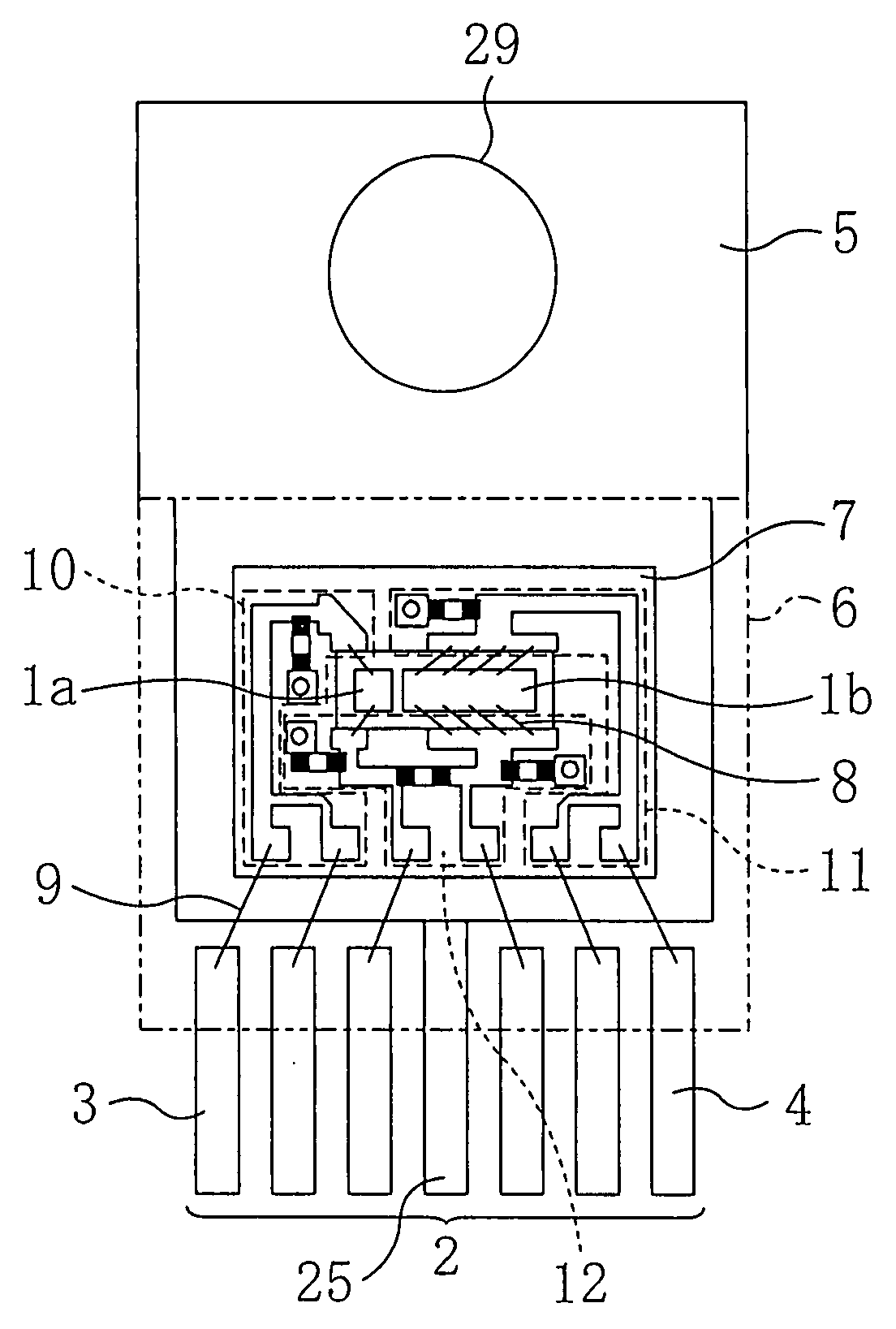
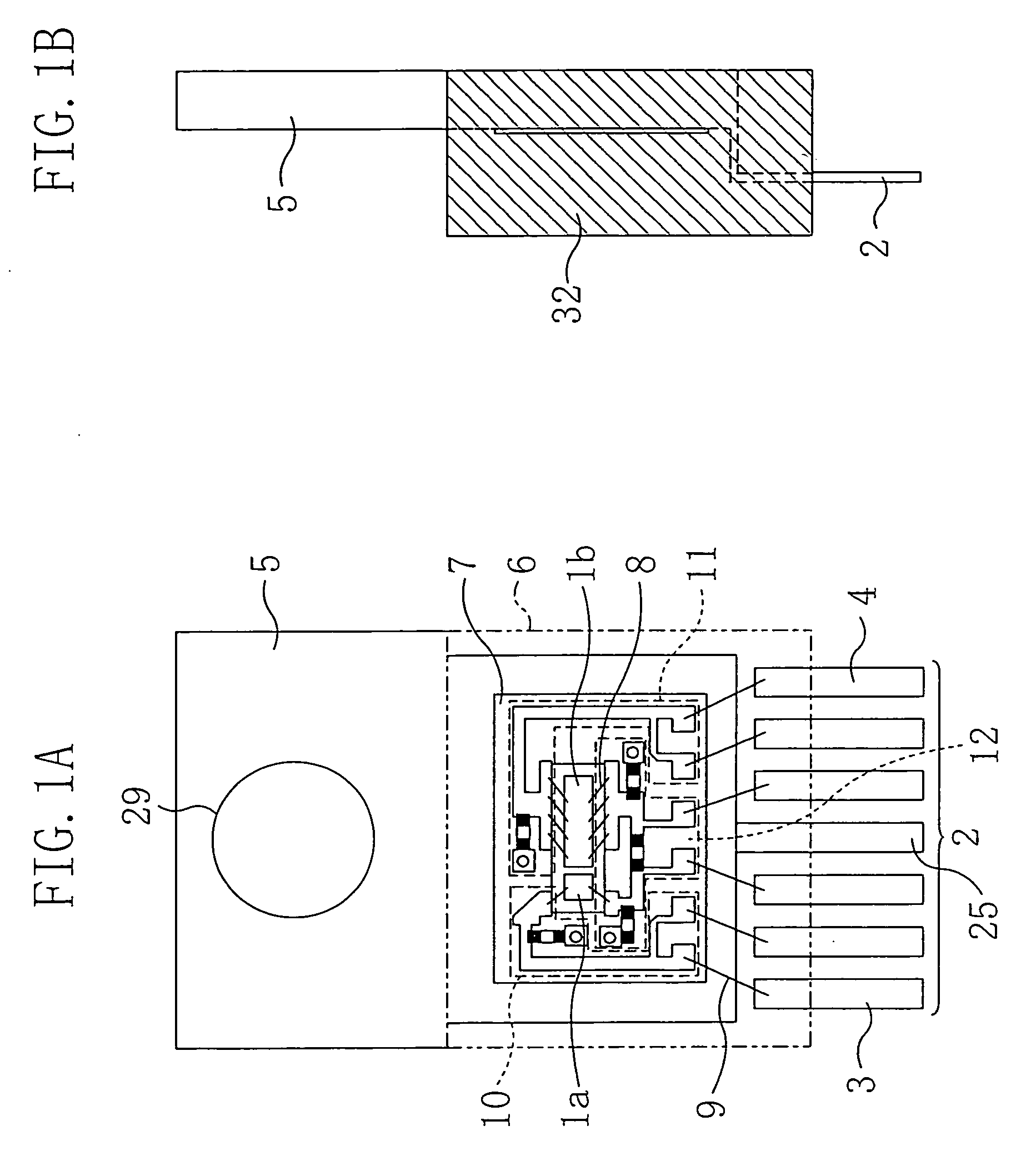
[0047]FIG. 1A is a view showing an example of the structure of a power amplifier module according to a first embodiment of the present invention, from which a mold resin has been removed. FIG. 1B is a view showing an example in which the power amplifier module according to the first embodiment is viewed from a side surface thereof. The power amplifier module according to the first embodiment has the function of amplifying a signal inputted to an input lead terminal 3 and outputting the amplified signal from an output lead terminal 4.

[0048] As shown in FIGS. 1A and 1B, the power amplifier module comprises: a plurality of external connection lead terminals 2 including the input lead terminal 3, the output lead terminal 4, and an RF grounding lead terminal 25; a heat dissipation plate 5 connected to the RF grounding lead terminal 25; first and second semiconductor devices 1a and 1b mounted on the heat dissipation plate 5; a printed circuit board 7 mounted on the heat dissipation plate...

embodiment 2

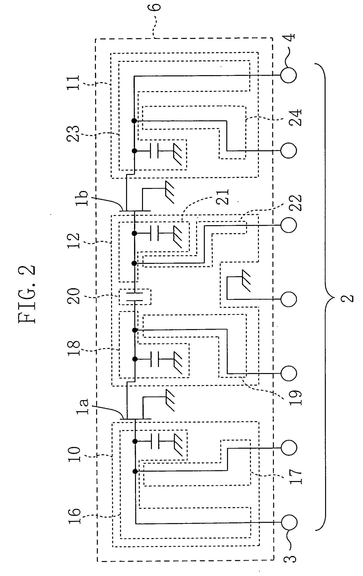
[0065]FIG. 4 is a view showing an example of the structure of a power amplifier module according to a second embodiment of the present invention, from which a mold resin has been removed. FIG. 5 is a circuit diagram showing an example of the power amplifier module according to the second embodiment.

[0066] In the power amplifier module according to the second embodiment, the first and second semiconductor devices 1a and 1b mounted on the power amplifier module according to the first embodiment are provided on the same semiconductor chip 13. When viewed from above, the five external connection lead terminals 2 are arranged within a range corresponding to the length of one edge of the mold resin and extending in the same direction. The center one of the external connection lead terminals 2 serves as the RF grounding lead terminal 25 connected to the heat dissipation plate 5. As for the other members shown in FIG. 4 which are the same as used in the power amplifier module according to ...

embodiment 3

[0076]FIG. 7 is a view showing an example of the structure of a power amplifier module according to a third embodiment of the present invention, from which a mold resin has been removed. FIG. 8 is a circuit diagram showing an example of the power amplifier module according to the third embodiment.

[0077] The power amplifier module according to the third embodiment has been obtained by reducing the number of the semiconductor devices to one in the power amplifier module according to the first embodiment.

[0078] In this case, only the input circuit portion 10 and the output circuit portion 11 are provided in the printed circuit board 7. The number of the external connection lead terminals 2 composing the power amplifier module according to the third embodiment can also be set to 5.

[0079] If the input lead terminal 3 and the input bias lead terminal of the semiconductor device 1 are formed as a common terminal and the output lead terminal 4 and the output bias lead terminal of the sem...


PUM


Abstract

A semiconductor device has a plurality of external connection lead terminals including an input lead terminal, an output lead terminal, and an RF grounding lead terminal, a heat dissipation plate connected to the RF grounding lead terminal, a semiconductor device and a printed circuit board each mounted on the heat dissipation plate, and a mold resin for sealing the semiconductor device, the printed circuit board, and the heat dissipation plate such that at least a part of the back surface of the heat dissipation plate is exposed. The semiconductor device amplifies a signal inputted to the input lead terminal and outputs the amplified signal from the output lead terminal.

Description

[0001] The present application claims priority under 35 U.S.C. § 119(a) to Japanese Patent Application JP 2004-269537, filed Sep. 16, 2004, the entire content of which is incorporated herein by reference. BACKGROUND OF THE INVENTION [0002] 1. Technical Field to Which the Invention Pertains [0003] The present invention relates to a power amplifier module and, more particularly, to a power amplifier module used for a transmission power amplifier provided at a base station for mobile communication equipment or the like. [0004] 2. Prior Art [0005] A power amplifier module has been used as a device composing a transmission power amplifier provided at a base station for mobile communication equipment. FIG. 12 is a view showing an example of the circuit structure of the transmission power amplifier provided at the base station for mobile communication equipment. FIG. 10A is a perspective view showing an example of the outer configuration of a conventional power amplifier module. FIG. 10B i...

Claims


Application Information

Patent Timeline
Patent Type & Authority Applications(United States)
IPC IPC(8): H01L23/34
CPCH01L23/36H01L23/49562H01L23/66H01L25/072H01L2223/665H01L2224/48091H01L2224/48247H01L2224/49171H01L2224/49175H01L2924/19041H01L2924/19107H01L2924/3011H05K3/0061H05K3/284H01L2924/00014H01L24/48H01L24/49H01L2924/00H01L2224/451H01L24/45
Inventor MIYAJI, MASAYUKINAGATA, SADAOTANIUCHI, HIROTADAOTA, YORITOIWAKIRI, TAKAHIROSAKATANI, TOMOTAKA
Owner PANASONIC CORP
Why Eureka
Try Eureka