
High-power and high-efficiency power amplifier insensitive to source impedance and load impedance

A power amplifier, load impedance technology, applied in power amplifiers, amplifiers, amplifiers with semiconductor devices/discharge tubes, etc., can solve the problems of low load impedance sensitivity, reduce power amplifier efficiency, and design difficulty, and achieve improvement. Power gain and power capacity, improve stability and reliability, reduce the effect of mutual limitation of indicators

Inactive Publication Date: 2018-03-27
CHENGDU GANIDE TECH
View PDF5 Cites 0 Cited by
  • Summary
  • Abstract
  • Description
  • Claims
  • Application Information

AI Technical Summary

Problems solved by technology

[0004] (1) Low load impedance sensitivity and high efficiency indicators in traditional balanced amplifiers restrict each other: since the output of the power amplifier in the microwave and millimeter wave front-end transmitter needs to be connected to an antenna with poor standing wave characteristics, the antenna is not suitable for microwave The low load impedance sensitivity of millimeter-wave power amplifiers poses a serious challenge; the existing balanced power amplifiers based on the Lange structure to achieve a 90° phase shift often introduce relatively high load impedance sensitivity in the input and output matching networks while improving the load impedance sensitivity. Large in-band insertion loss, thereby reducing the efficiency of the power amplifier; the load impedance sensitivity and output power of the existing balanced power amplifier based on the dual phase shift structure to achieve a phase shift of ±45° still have a large room for improvement
Therefore, low load impedance sensitivity and high efficiency indicators in existing balanced amplifiers are mutually restricted
[0005] (2) It is difficult to design high-power and high-gain indicators of traditional balanced amplifiers in the microwave and millimeter wave bands: driven by the future 5G market, microwave and millimeter wave front-end transmitters urgently need high gain, high power, high efficiency, and low load impedance sensitivity. high-degree power amplifier, but the existing millimeter-wave frequency band application circuit must use a semiconductor process transistor with a small gate length. Due to the influence of its low breakdown voltage, the voltage swing of the power amplifier will be greatly limited, so it is also Limits the power capability of the power transistor
[0008] In order to improve the low load impedance sensitivity of the circuit, the designer often needs to use the Lange structure to achieve a 90° phase shift of the two balanced structure signals, and also reduce the introduced in-band loss as much as possible, while ensuring that the two balanced signals have Approximately the same in-band loss, in addition, it is necessary to cooperate with other matching structures to achieve impedance matching between the input of the transistor and the input port, which greatly increases the complexity and difficulty of circuit design
In order to compromise various design indicators, designers often need to introduce a certain in-band loss to achieve a 90° phase shift and impedance matching, which greatly reduces the efficiency indicators of the power amplifier.
[0009] (2) It is difficult to match the impedance of high-power transistors in the millimeter wave band
[0010] Since the amplifier works in the millimeter wave band, the power capacity of a single transistor is limited. In order to obtain a higher power capacity, the designer often needs a 2n times power combining structure. This structure often leads to a very low optimal load impedance of the output network, which is This kind of low load impedance will make the impedance matching of microwave and millimeter wave band balanced amplifiers more difficult

Method used


Image

  • High-power and high-efficiency power amplifier insensitive to source impedance and load impedance
  • High-power and high-efficiency power amplifier insensitive to source impedance and load impedance

Examples


Embodiment Construction

[0032] Exemplary embodiments of the present invention will now be described in detail with reference to the accompanying drawings. It should be understood that the implementations shown and described in the drawings are only exemplary, intended to explain the principle and spirit of the present invention, rather than limit the scope of the present invention.

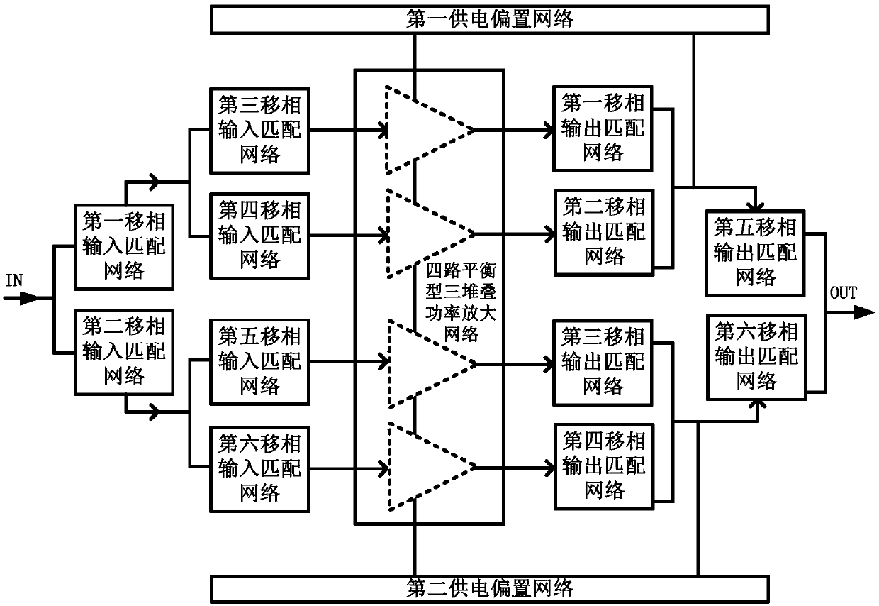
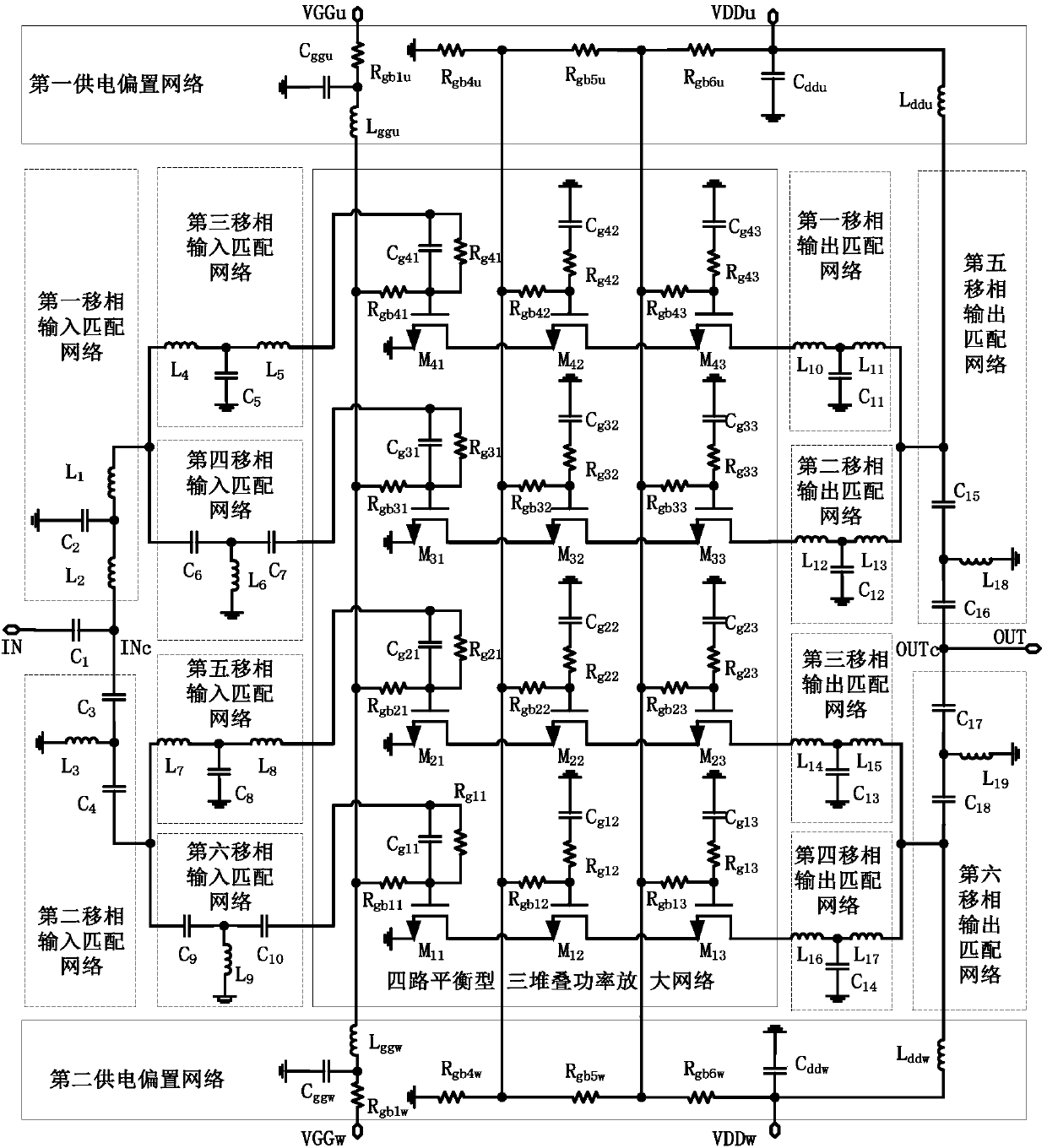
[0033] Embodiments of the present invention provide a high-power and high-efficiency power amplifier that is insensitive to source and load impedances, such as figure 1 As shown, including the first phase-shifting input matching network, the second phase-shifting input matching network, the third phase-shifting input matching network, the fourth phase-shifting input matching network, the fifth phase-shifting input matching network, the sixth phase-shifting input matching network network, four-way balanced three-stack power amplifying network, the first phase-shift output matching network, the second phase-shift output ma...


PUM


Abstract

The invention discloses a high-power and high-efficiency power amplifier insensitive to source impedance and load impedance. An amplification function of a balance type amplifier is realized through adoption of four ways of three-stack transistor amplification networks, the power gain and power capacity of the balance type amplifier are greatly improved; and moreover, + / -45-degree and + / -135-degree phase-shifting control and input and output impedance matching of four ways of balance signals are realized through utilization of a multi-level T-type filtering phase shift circuit, so on the premise of low insertion loss and high efficiency, the sensitivity of the amplifier for the source impedance and the load impedance is greatly reduced, and the circuit stability and robustness are improved. According to the high-power and high-efficiency power amplifier insensitive to the source impedance and the load impedance realized by the invention, the output power is high, the power gain is high, and the low load impedance sensitivity is high.

Description

technical field [0001] The invention belongs to the technical field of field effect transistor microwave millimeter wave power amplifier and integrated circuit, and specifically relates to the design of a high-power and high-efficiency power amplifier insensitive to source and load impedance. Background technique [0002] With the rapid development of 3G, 4G-LTE and other civilian communication markets, as well as the early layout of 5G communication, microwave and millimeter wave front-end transmitters are also developing in the direction of high power, high integration, and high efficiency in microwave and millimeter wave bands; in addition, due to MIMO With the wide application of technology, the system poses a severe test to the load impedance sensitivity of the terminal power amplifier. Therefore, the market urgently needs low load impedance sensitivity, high power, and high efficiency power amplifier chips for microwave and millimeter wave frequency bands. [0003] How...

Claims


Application Information

Patent Timeline
IPC IPC(8): H03F1/56H03F3/21H03F3/24H03G3/30
CPCH03F1/56H03F3/21H03F3/245H03G3/3042
Inventor 胡柳林邬海峰滑育楠廖学介陈依军吕继平童伟王测天吴曦杨云婷
Owner CHENGDU GANIDE TECH
Learn More