Structures for Reducing Electron Concentration and Process for Reducing Electron Concentration

a technology of electron concentration and structure, applied in the field of transistors, can solve the problems of limited group iii-nitride hemts, and achieve the effects of reducing electron concentration, increasing power gain, and increasing efficiency

Active Publication Date: 2020-09-24
WOLFSPEED INC
View PDF0 Cites 6 Cited by
  • Summary
  • Abstract
  • Description
  • Claims
  • Application Information

AI Technical Summary

Benefits of technology

[0005]One general aspect includes a device including: a substrate. The device also includes a buffer layer on the substrate. The device also includes a barrier layer on the buffer layer. The device also includes a source electrically coupled to the barrier layer. The device also includes a gate electrically coupled to the barrier layer. The device also includes a drain electrically coupled to the barrier layer; and an electron concentration reduction structure arranged with at least one of the following: in the barrier layer and on the barrier layer, where the electron concentration reduction structure is configured to at least one of the following: reduce electron concentration around the gate, reduce electron concentration around an edge of the gate, reduce electron concentration, such as between the gate and the drain and / or between the gate and the source, increase power gain, increase efficiency, decouple the gate from the drain, decouple the gate from the source, and reduce capacitance, such as the capacitance between the gate and the drain and / or between the gate and the source.

Problems solved by technology

However, Group III-nitride HEMTs can be limited by a high gate drain capacitance, a high gate source capacitance, and / or other capacitances induced by the high electron concentration around the gate.

Method used


Image

  • Structures for Reducing Electron Concentration and Process for Reducing Electron Concentration
  • Structures for Reducing Electron Concentration and Process for Reducing Electron Concentration
  • Structures for Reducing Electron Concentration and Process for Reducing Electron Concentration

Examples


Embodiment Construction

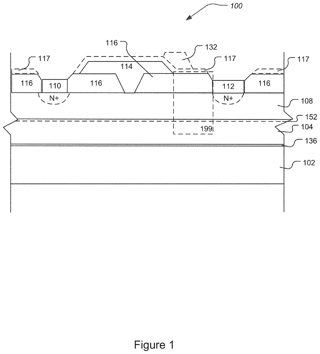
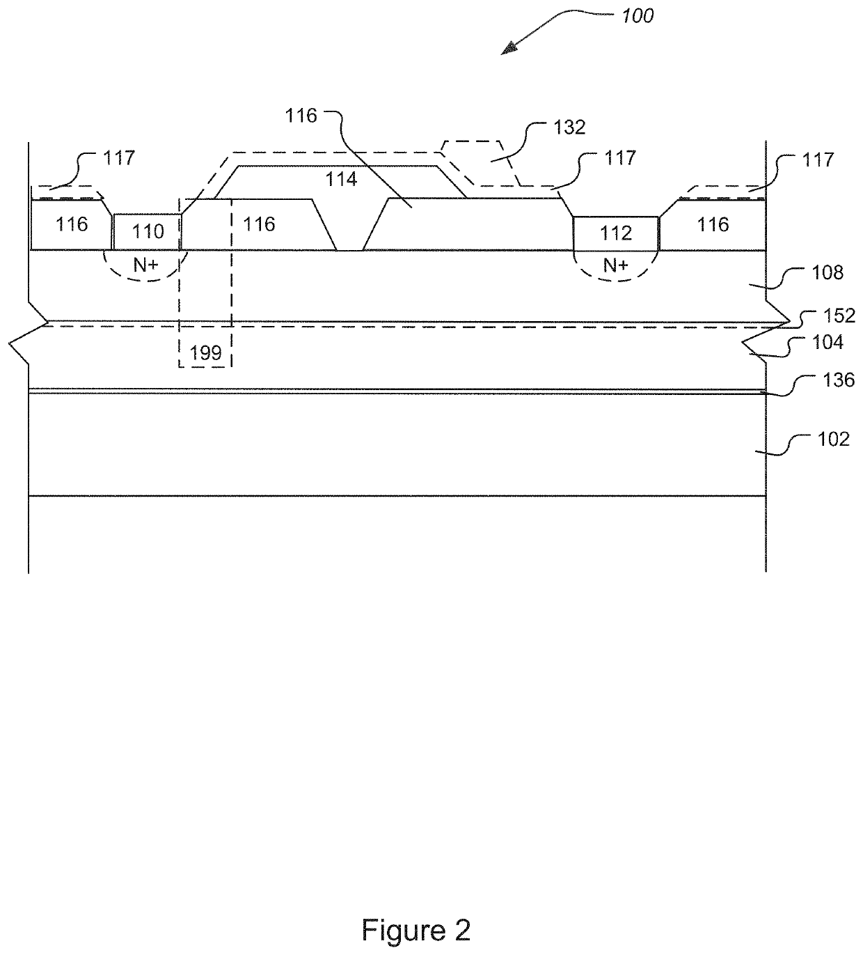
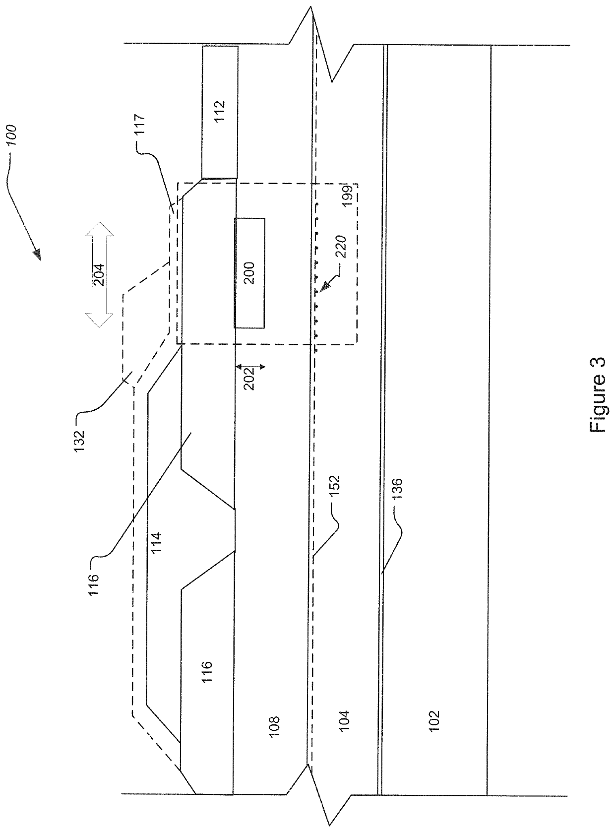
[0020]The aspects of the disclosure and the various features and advantageous details thereof are explained more fully with reference to the non-limiting aspects and examples that are described and / or illustrated in the accompanying drawings and detailed in the following description. It should be noted that the features illustrated in the drawings are not necessarily drawn to scale, and features of one aspect may be employed with other aspects as the skilled artisan would recognize, even if not explicitly stated herein. Descriptions of well-known components and processing techniques may be omitted so as to not unnecessarily obscure the aspects of the disclosure. The examples used herein are intended merely to facilitate an understanding of ways in which the disclosure may be practiced and to further enable those of skill in the art to practice the aspects of the disclosure. Accordingly, the examples and aspects herein should not be construed as limiting the scope of the disclosure, ...


PUM

PropertyMeasurementUnit
depthaaaaaaaaaa
depthaaaaaaaaaa
depthaaaaaaaaaa

Abstract

A device includes a substrate; a buffer layer on the substrate; a barrier layer on the buffer layer, a source electrically coupled to the barrier layer; a gate electrically coupled to the barrier layer; and a drain electrically coupled to the barrier layer. The device further includes an electron concentration reduction structure arranged with at least one of the following: in the barrier layer and on the barrier layer. The electron concentration reduction structure is configured to at least one of the following: reduce electron concentration around the gate, reduce electron concentration around an edge of the gate, reduce electron concentration, increase power gain, increase efficiency, decouple the gate from the drain, decouple the gate from the source, and reduce capacitance.

Description

FIELD OF THE DISCLOSURE[0001]The disclosure relates to transistors having structures for reducing gate adjacent electron concentration for increasing power gain and efficiency. The disclosure also relates to a process for reducing gate adjacent electron concentration for increasing power gain and efficiency in transistors.BACKGROUND OF THE DISCLOSURE[0002]Group III-nitride based high-electron mobility transistors (HEMTs) are very promising candidates for high power amplifiers, radiofrequency (RF) applications, and also for low frequency high power switching applications since the material properties of Group III-nitrides, such as gallium nitride (GaN) and its alloys enable achievement of high voltage and high current along with high RF gain and linearity for RF applications. A typical Group III-nitride HEMT comprises a substrate, a Group III-nitride (e.g., GaN) buffer or channel layer formed on the substrate, and a higher band-gap Group III-nitride (e.g., AlGaN) formed on the buffer...

Claims


Application Information

Patent Timeline
Patent Type & Authority Applications(United States)
IPC IPC(8): H01L29/778H01L29/66H01L29/06
CPCH01L29/66462H01L29/0607H01L29/7786H01L29/402H01L29/42316H01L29/32H01L29/0657H01L29/0619H01L29/2003H01L29/0843H01L29/207
Inventor GUO, JIASHEPPARD, SCOTTSRIRAM, SAPTHARISHI
Owner WOLFSPEED INC
Why Eureka
Try Eureka