High gain V wave band power amplifier based on genetic algorithm optimization

A technology of power amplifiers and genetic algorithms, applied in genetic rules, multi-objective optimization, instruments, etc., can solve the problems of circuit center frequency band and matching performance deviation, low Q value of passive devices, large area, etc., to achieve chip area reduction, Ease of implementation and integration, small circuit area effect

Inactive Publication Date: 2018-09-21
CHONGQING UNIV OF POSTS & TELECOMM
View PDF6 Cites 6 Cited by
  • Summary
  • Abstract
  • Description
  • Claims
  • Application Information

AI Technical Summary

Problems solved by technology

The disadvantage of the first solution is that the Q value of passive components in the existing component library is low; the disadvantage of the second solution is that the loss is large and the area is large; the third solution can reduce the area,

Method used


Image

  • High gain V wave band power amplifier based on genetic algorithm optimization
  • High gain V wave band power amplifier based on genetic algorithm optimization
  • High gain V wave band power amplifier based on genetic algorithm optimization

Examples


Embodiment Construction

[0037] The technical solutions in the embodiments of the present invention will be described clearly and in detail below with reference to the drawings in the embodiments of the present invention. The described embodiments are only some of the embodiments of the invention.

[0038]The technical scheme that the present invention solves the problems of the technologies described above is:

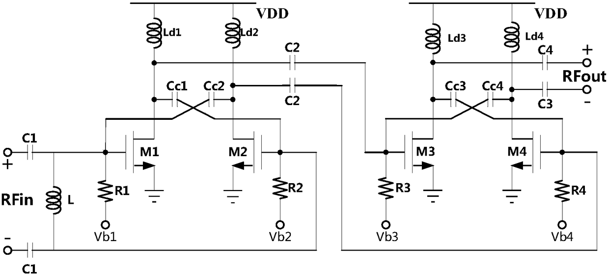
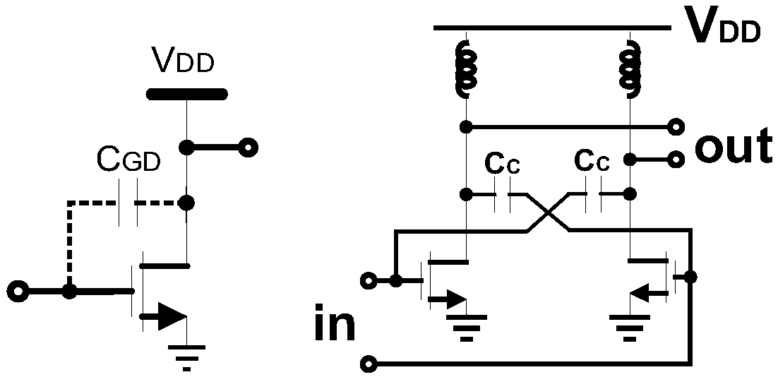
[0039] Such as figure 1 As shown, the present invention adopts the design of the high-gain V-band power amplifier optimized by cross-coupling capacitor and genetic algorithm. The circuit structure includes an input matching network, a first-stage pseudo-differential common-source amplifier, an inter-stage matching network, a second-stage pseudo-differential common-source amplifier, and an output matching network. The input terminal of the input matching network is connected to the signal source or power source (Vs), the output terminal of the input matching network is connected to the input...


PUM


Abstract

The invention discloses a high gain V wave band power amplifier based on genetic algorithm optimization. The power amplifier comprises two stages of pseudo differential common source structures whichare in tandem connection successively, and the pseudo differential common-source amplifier structures adopt the cross coupling capacitance neutralization technology; the input-stage matching network adopts a series capacitance shunt inductance mode; two stages of amplifiers directly adopt a capacitance direct coupling link for matching. A shunt inductance is adopted in the input-stage matching network so that matching network loss can be reduced; in addition, the cross coupling capacitance neutralization is adopted to improve power gain, improve circuit reverse isolation and stability, and achieve high gain under the circumstance of not increasing extra power dissipation. In order to solve the center frequency and matching performance deviation theoretical value caused by element parasitism, the genetic algorithm is adopted to slightly adjust sizes of passive devices (inductances) and CMOS transistors so that the circuit can reach the optimum performance under the parasitic effect influence. The circuit designed by the power amplifier is simple in structure and easy to design and implement.

Description

technical field [0001] The invention belongs to the field of electronic technology and relates to the design of a microwave power amplifier, in particular to a high-gain V-band power amplifier designed based on a 90nm CMOS process with a cross-coupling capacitor structure and optimized by a genetic algorithm. It should be noted that the design method of the microwave power amplifier involved in this invention is not limited to the 90nm CMOS process, but is also applicable to other deep submicron CMOS process technology nodes. Background technique [0002] At present, because the power amplifier using the RF_CMOS process has the characteristics of high integration and easy combination with the baseband CMOS circuit, and with the advancement of deep submicron CMOS process technology, the characteristic frequency of the RF_CMOS transistor exceeds 100GHz, so the microwave power based on RF_CMOS technology The design of amplifiers has received more and more attention. However, t...

Claims


Application Information

Patent Timeline
IPC IPC(8): G06F17/50G06N3/12
CPCG06N3/126G06F30/36G06F2111/06
Inventor 王巍黄孟佳杨皓李双巧王伊昌袁军
Owner CHONGQING UNIV OF POSTS & TELECOMM
Why Eureka
Try Eureka