Pre-packaged structure

Inactive Publication Date: 2011-04-07
ANPEC ELECTRONICS CORPORATION
View PDF4 Cites 3 Cited by
  • Summary
  • Abstract
  • Description
  • Claims
  • Application Information

AI Technical Summary

Benefits of technology

[0012]Because the pre-packaged structure of the present invention provides a buffer metal layer which is thick enough on the top surface of the die, there is no needed to concern the overwhelming stress of the wire bonding for fixing the wires onto the electric points above the core circuit and the potential c

Problems solved by technology

Although the force needed by the gold wires is within the limit of the core circuit 121, gold is however on one hand much more expensive than copper and on the other hand, the electrical resistance of gold is still higher than that of copper, this solution is as a result di

Method used


Image

  • Pre-packaged structure
  • Pre-packaged structure
  • Pre-packaged structure

Examples


Example

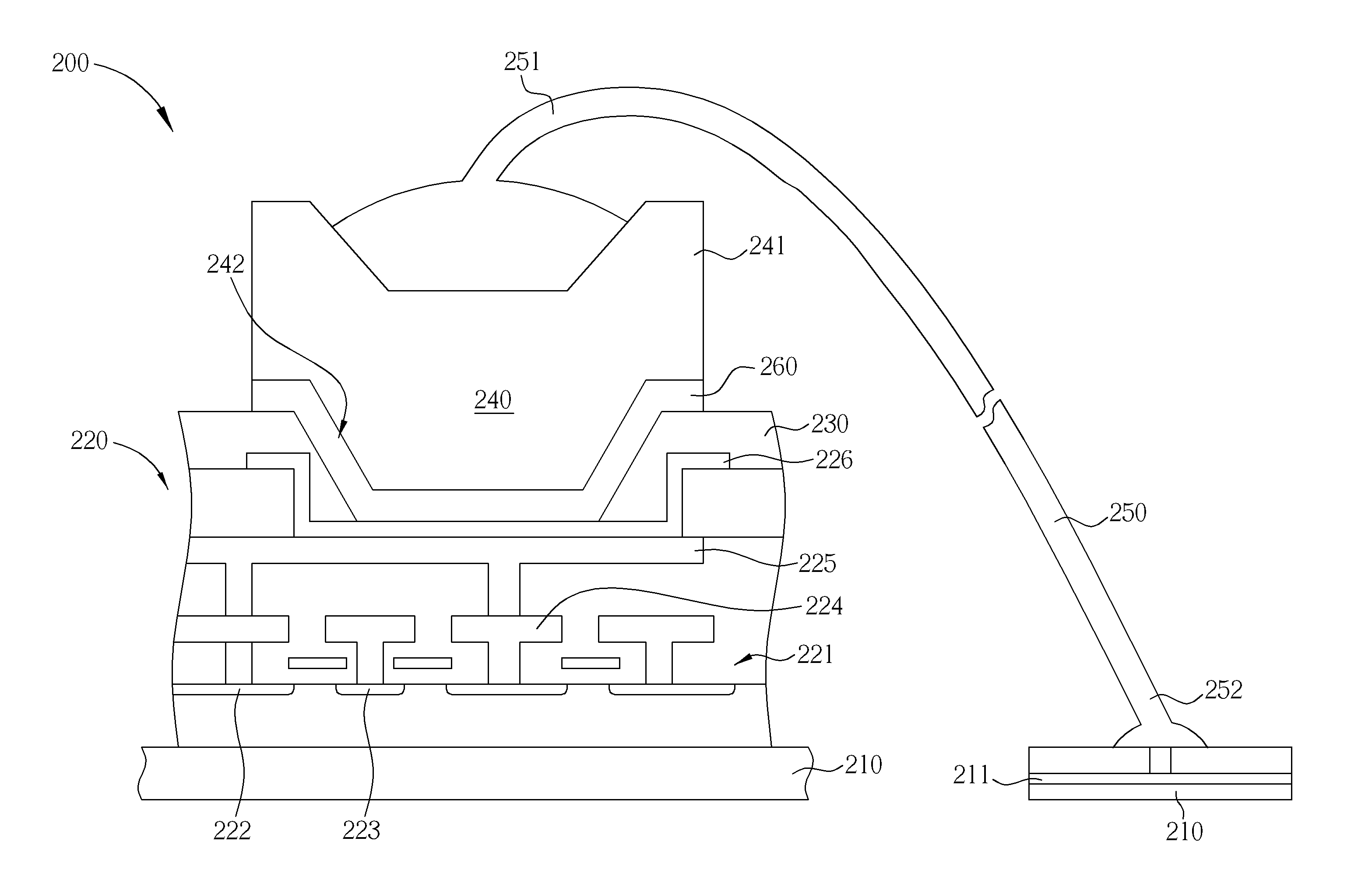
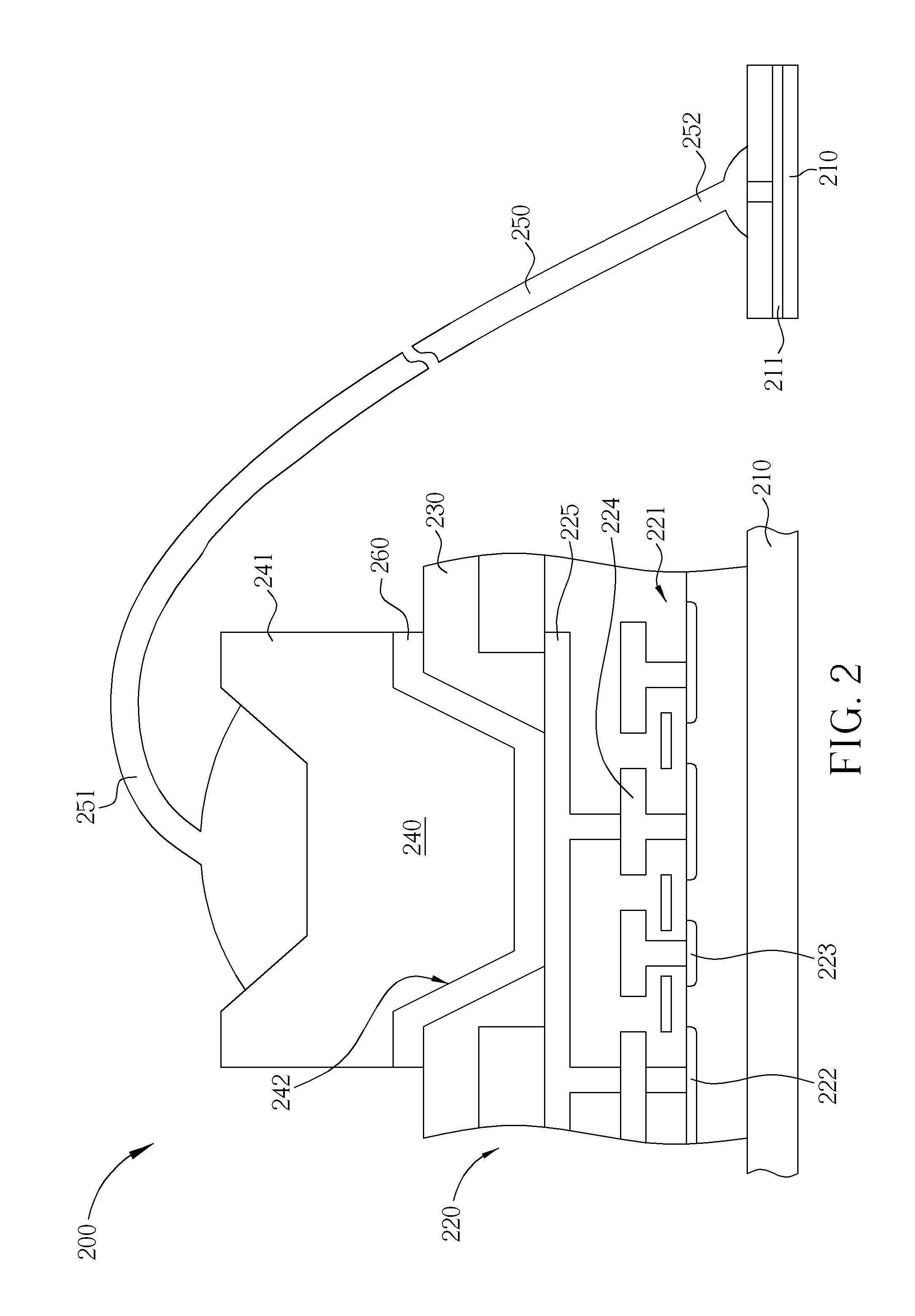
[0017]The present invention in one aspect provides a novel pre-packaged structure. In the pre-packaged structure of the present invention, a layer of buffer metal which is thick enough is provided on the top surface of the die to shield the overwhelming stress which is caused by wire bonding for fixing the wire bonds onto the electric points above the core circuit and to avoid the potential cracks and substantial damages to the underlying core circuit. In another aspect, the pre-packaged structure of the present invention also allows the copper wire to directly electrically contact the electric points of the core circuit so that one end of the copper wires is directly disposed right above the core circuit. In such a way, the gold wires, which are expensive and have higher electrical resistance, are no longer needed to take advantage of a lower production cost.

[0018]The present invention first provides a novel pre-packaged structure. Please refer to FIG. 2, illustrating an embodiment...


PUM


Abstract

A pre-packaged structure includes a substrate with a substrate circuit, a die having a core circuit and disposed on the substrate, a passivation selectively covering the core circuit, a buffer metal layer electrically connected to the core circuit and completely covering the passivation and a copper wire bond electrically connected to the buffer metal layer and the substrate circuit.

Description

BACKGROUND OF THE INVENTION[0001]1. Field of the Invention[0002]The present invention generally relates to a pre-packaged structure. In particular, the present invention is directed to a pre-packaged structure so that a copper wire can be directly disposed in the pre-packaged structure and right on the core circuit within.[0003]2. Description of the Prior Art[0004]In order to meet the demands of “light, small, short and thin” characteristics for electronic products, the technology of packaging is progressing. During the advancing progress of the technology of packaging, many techniques are developed, such as wire bonding or flip-chip.[0005]Please refer to FIG. 1, which illustrates a conventional technology of packaging. The conventional technology of packaging usually requires a chip substrate 110 to support and to connect at least one die 120 or other packaging element(s) to be packaged to form a chip, which can be further electrically connected to a circuit such as a motherboard (...

Claims


Application Information

Patent Timeline
IPC IPC(8): H01L23/49
CPCH01L24/05H01L2924/00015H01L24/48H01L24/73H01L2224/04042H01L2224/05082H01L2224/05556H01L2224/05558H01L2224/05647H01L2224/45147H01L2224/4807H01L2224/48091H01L2224/48227H01L2224/48247H01L2224/4845H01L2224/48465H01L2924/01028H01L2924/01029H01L2924/01047H01L2924/01075H01L2924/01079H01L2924/3025H01L24/45H01L2224/48647H01L2224/48847H01L2924/01033H01L2224/02166H01L2224/45144H01L2924/00014H01L2924/00
Inventor TSAI, SHIH-WEICHANG, HSIANG-CHUNG
Owner ANPEC ELECTRONICS CORPORATION
Why Eureka
Try Eureka