3D integrated circuit layer interconnect

a technology of integrated circuit layer and interconnection structure, which is applied in the direction of semiconductor devices, semiconductor/solid-state device details, electrical apparatus, etc., can solve the problems of increasing the cost of interconnection implementation, reducing the memory density, and increasing the cost per bit, so as to achieve efficient and low-cost manufacturing methods

Active Publication Date: 2011-04-14
MACRONIX INT CO LTD
View PDF11 Cites 64 Cited by
  • Summary
  • Abstract
  • Description
  • Claims
  • Application Information

AI Technical Summary

Benefits of technology

[0011]A 3D interconnect structure with a small footprint is described, useful for connection from above to levels of circuit structures in a multi-level device. Also, an efficient and low cost method for manufacturing the 3D interconnect structure is provided.

Problems solved by technology

Also, the cost to implement the interconnections increases with the number of lithographic steps needed.
This results in significantly smaller memory areas in the upper levels, reducing the memory density and increasing the cost per bit.
Also, there is a practical limit to the number of levels that can be layered in this way.
Thus, although the benefits of higher density are achieved using three-dimensional stacked memory, the reduced memory density and resulting higher per bit manufacturing costs for the upper layers limit the use of the technology.

Method used


Image

  • 3D integrated circuit layer interconnect
  • 3D integrated circuit layer interconnect
  • 3D integrated circuit layer interconnect

Examples


Embodiment Construction

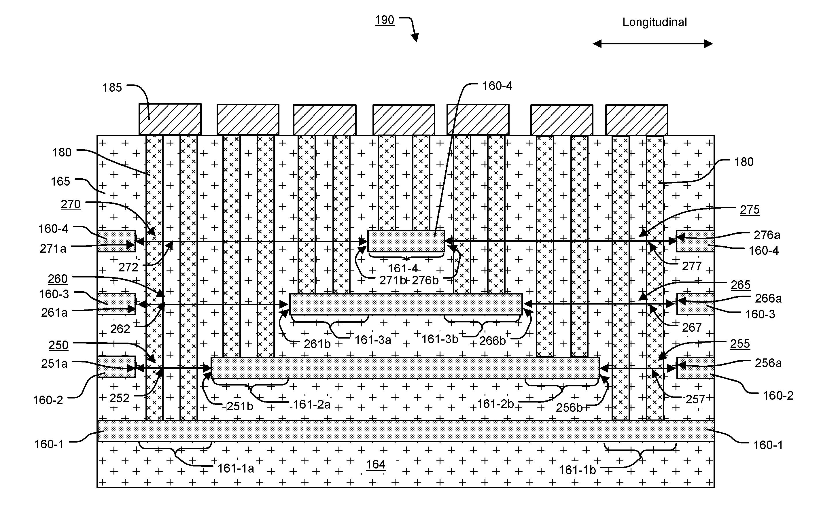
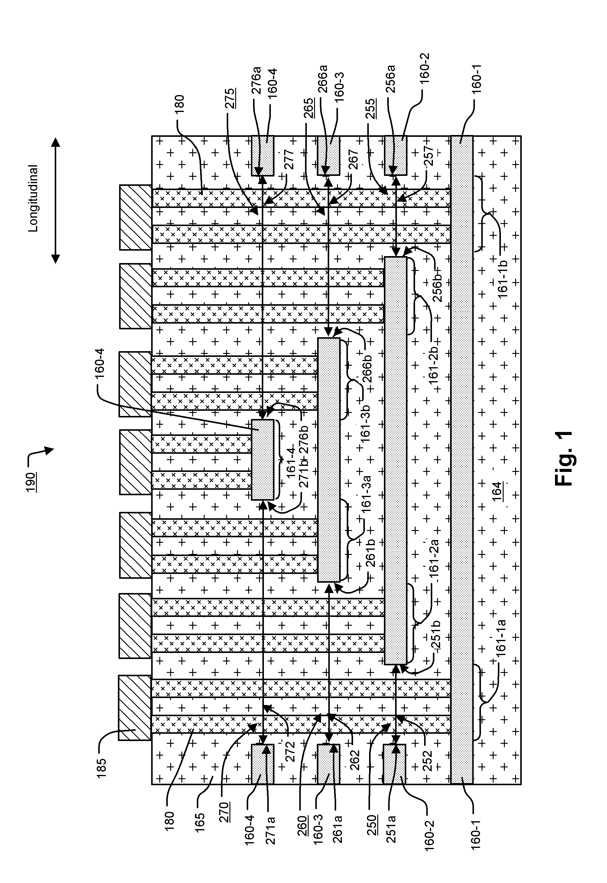
[0042]A detailed description of embodiments of the present invention is provided with reference to the FIGS. 1-16.

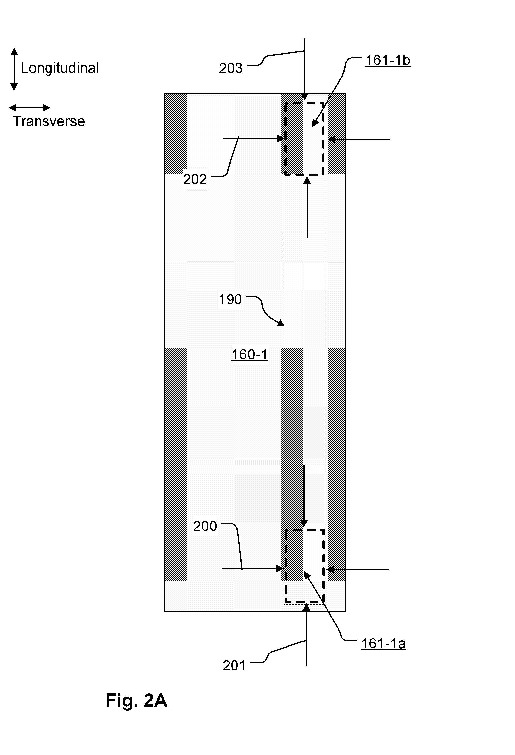
[0043]FIG. 1 illustrates a cross-sectional view of a device including three-dimensional structure having an interconnect structure 190 with a small footprint where conductors 180 extend to various levels 160-1 to 160-4 in the device. In the illustrated example four levels 160-1 to 160-4 are shown. More generally, the small interconnect structure 190 described herein can be implemented in a structure having levels 0 to N, where N is at least 2.

[0044]The conductors 180 are arranged within the interconnect structure 190 to contact landing areas on the various levels 160-1 to 160-4. As described in more detail below, the conductors 180 for each particular level extend through openings in the overlying levels to contact the landing areas 161-1a, 161-1b, 161-2a, 161-2b, 161-3a, 161-3b, 161-4. The conductors 180 are used in this example for coupling the levels 160-1 to 160-4 to...


PUM


Abstract

A three-dimensional 3D interconnect structure with a small footprint is described, useful for connection from above to levels of circuit structures in a multi-level device. Also, an efficient and low cost method for manufacturing the 3D interconnect structure is provided.

Description

BACKGROUND OF THE INVENTION[0001]1. Field of the Invention[0002]The present invention relates generally to high density integrated circuit devices, and more particularly to interconnect structures for multi-level three-dimensional stacked devices.[0003]2. Description of Related Art[0004]In the manufacturing of high density memory devices, the amount of data per unit area on an integrated circuit can be a critical factor. Thus, as the critical dimensions of the memory devices approach lithographic technology limits, techniques for stacking multiple levels of memory cells have been proposed in order to achieve greater storage density and lower costs per bit.[0005]For example, thin film transistor techniques are applied to charge trapping memory in Lai, et al., “A Multi-Layer Stackable Thin-Film Transistor (TFT) NAND-Type Flash Memory”, IEEE Int'l Electron Devices Meeting, 11-13 Dec. 2006; and in Jung et al., “Three Dimensionally Stacked NAND Flash Memory Technology Using Stacking Sing...

Claims


Application Information

Patent Timeline
Patent Type & Authority Applications(United States)
IPC IPC(8): H01L23/535H01L21/768
CPCH01L23/522H01L27/0207H01L27/105H01L27/11206H01L27/11286H01L2924/0002H01L27/1052H01L2924/00H01L27/0688H10B99/00H10B20/20H10B20/60
Inventor LUNG, HSIANG-LAN
Owner MACRONIX INT CO LTD
Why Eureka
Try Eureka