
Architecture for controlling clock characteristics

Active Publication Date: 2011-04-14
CYCLOS SEMICON
View PDF99 Cites 67 Cited by
  • Summary
  • Abstract
  • Description
  • Claims
  • Application Information

AI Technical Summary

Benefits of technology

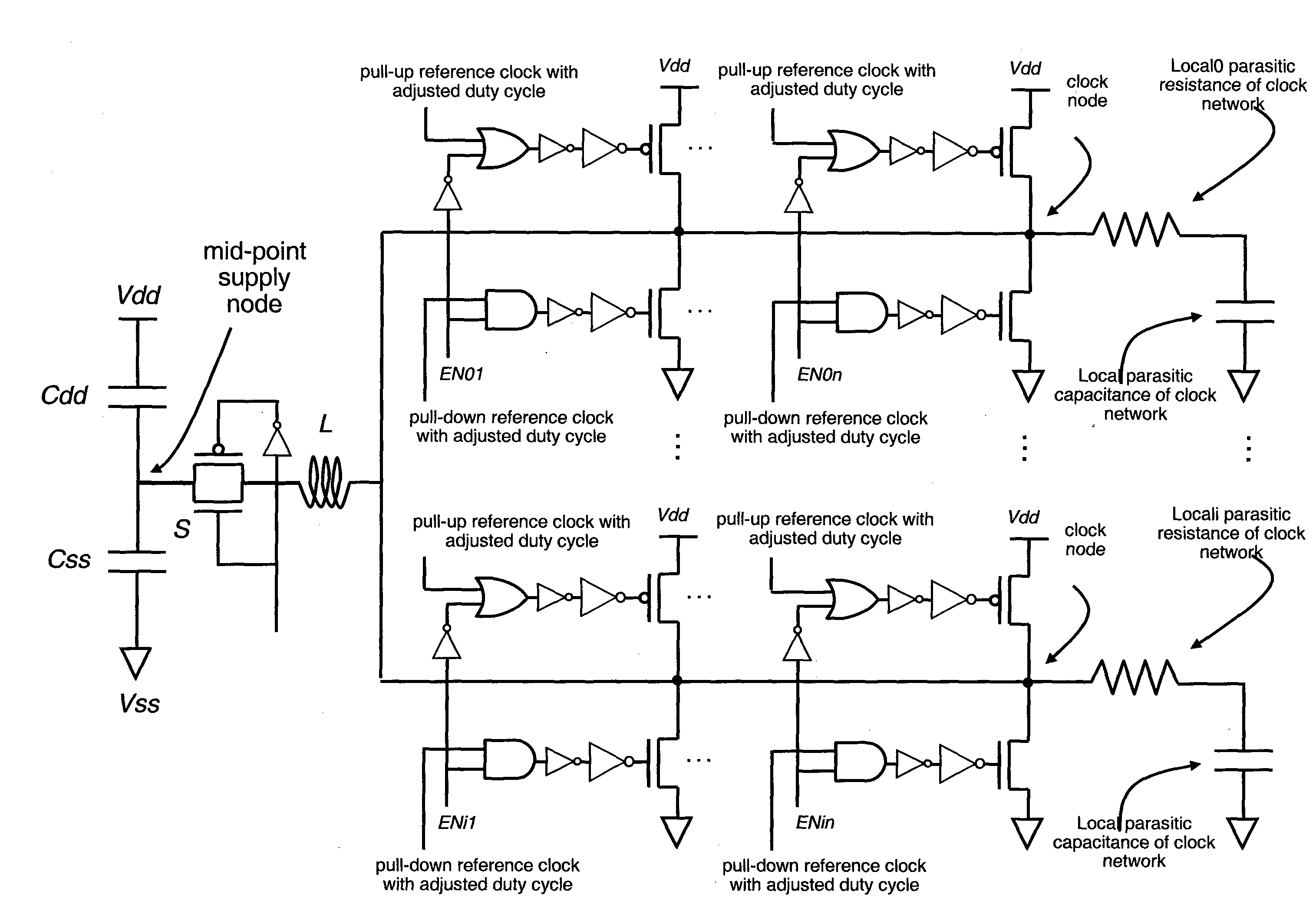
[0013]An architecture for controlling the clock waveform characteristics, including but not limited to the clock amplitude and clock rise and/or fall times, of resonant clock distribution networks is proposed. This architecture relies on controlling the size of clock drivers and the duty cycles of reference clocks. It is generally applicable to semiconductor devices with multiple clock frequencies, and high-performance and low-power clocking requirements such as microprocessors, ASICs, and SOCs. In some embodiments, the architecture can be realized with no need for routing additional power grids or additional control signals to clock-distribution network components whose physical locations are not

Problems solved by technology

Furthermore, clock distribution networks tend to be significant sources of energy consumption in high-performance designs, as they usually include over-sized devices to ensure that they conform to their specified characteristics under all anticipated variations of fabrication and operational conditions.
Consequently, in designs where it is desirable to minimize energy consumption, the design of clock distribution networks is especially challenging, because reductions in energy consumption of the clock distribution network will tend to negatively impact the ability of the clock distribution network to attain its specified characteristics.
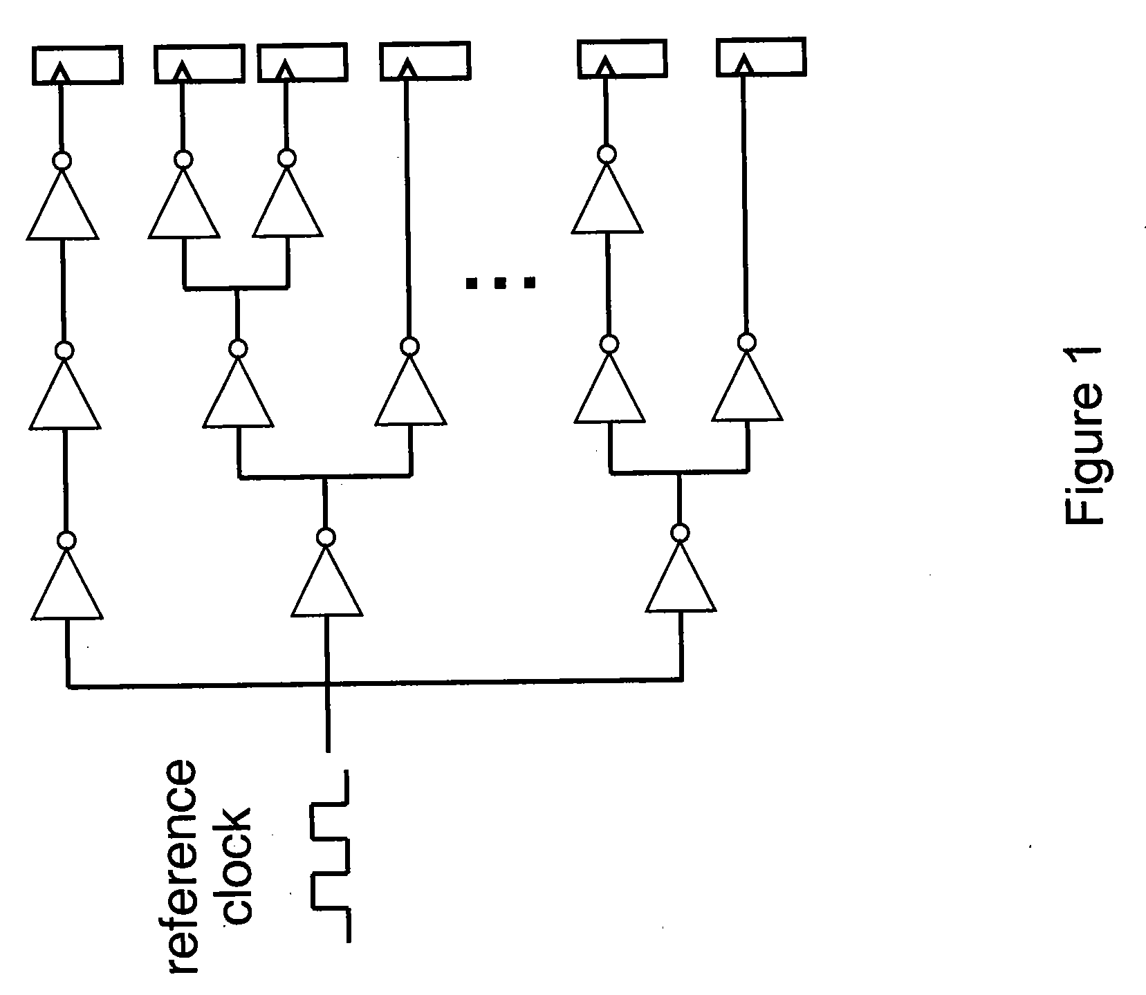
In particular, the sizes of the buffers are typically made large enough to insure that the rise times and fall times of these clock signals cannot exceed a certain upper bound, because many types of storage elements will not attain their specified performance characteristics if the rise and / or fall times are too long.
These final buffers are typically large and draw large amounts of current within a relatively small window of time.
These large current draws over a small time window can overwhelm the ability of the device's power-supply system, and cause variations in the voltage supplied to the final drivers, negatively impacting their performance.
Moreover, since the final drivers typically share the power-supply system with other parts of the overall device, any variations in voltage that they cause will affect the operation of other parts of the device, and have additional negative impacts.
Unfortunately, reduction of the voltage supplied to the clock distribution network buffers and reduction of the sizes of the transistors used to implement the buffers will have a negative impact on the ability of the network to realize suitable rise and / or fall times. Longer rise and / or fall times will generally have a negative impact on the performance of the storage elements that use the clock signal.
Moreover, since a reduction in the power-voltage supplied to the buffers will typically directly translate into a reduction in the peak-to-peak “swing” of the voltage of the clock signal itself, the performance of the storage elements that use the clock signal will further be negatively impacted.
However, if the clock buffers are on the same supply grid as the other circuitry in the device, the peak-to-peak voltage swing of the clock signal and rise and / or fall times of the clock signal may be so compromised by the low power-voltage, that performance of the storage elements using the clock will be too poor to be practical.
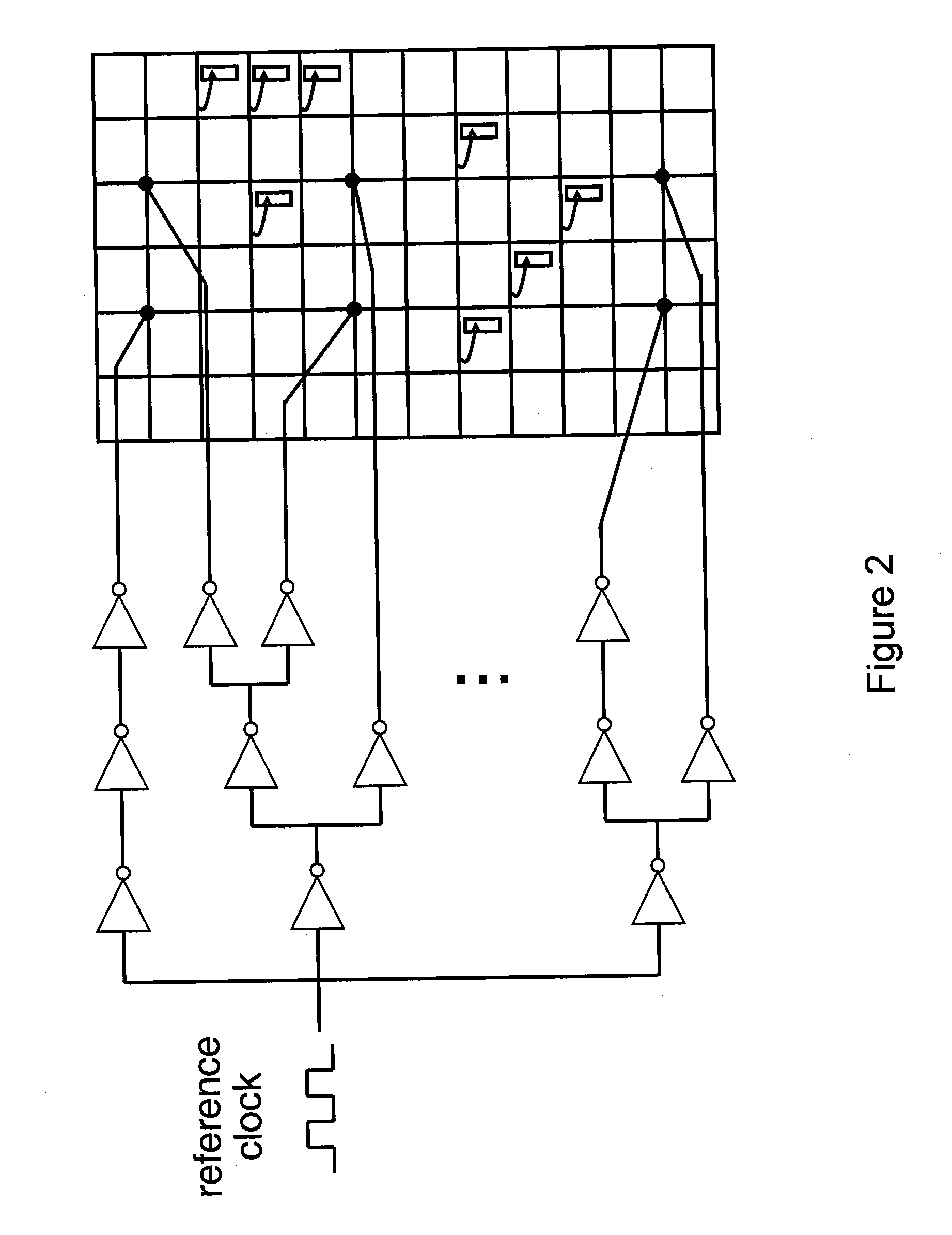
Such a separate supply grid would traditionally need to be distributed across the entire design, however, due to the distributed nature of the buffers in the distribution network, and thus, represents an amount of additional metal-interconnection resources that is not practical in many designs.
Overall network performance depends on operating speed and total network inductance, resistance, size, and topology, with lower-resistance symmetric networks resulting in lower jitter, skew, and energy consumption when designed with adequate inductance.
Moreover, they are not used to impact overall power consumption in the device by operating the clock signal at a higher or lower voltage than the other circuitry in the device, with the objective of achieving higher performance at a target voltage level, or lower energy consumption at a target performance level.

Method used


Image

  • Architecture for controlling clock characteristics
  • Architecture for controlling clock characteristics
  • Architecture for controlling clock characteristics

Examples


Embodiment Construction

[0027]Various examples of the invention will now be described. The following description provides specific details for a thorough understanding and enabling description of these examples. One skilled in the relevant art will understand, however, that the invention may be practiced without many of these details. Likewise, one skilled in the relevant art will also understand that the invention can include many other obvious features not described in detail herein. Additionally, some well-known structures or functions may not be shown or described in detail below, so as to avoid unnecessarily obscuring the relevant description.

[0028]The terminology used below is to be interpreted in its broadest reasonable manner, even though it is being used in conjunction with a detailed description of certain specific examples of the invention. Indeed, certain terms may even be emphasized below; however, any terminology intended to be interpreted in any restricted manner will be overtly and specific...


PUM


Abstract

An architecture for controlling the clock waveform characteristics, including but not limited to the clock amplitude and clock rise and / or fall times, of resonant clock distribution networks is proposed. This architecture relies on controlling the size of clock drivers and the duty cycles of reference clocks. It is targeted at resonant clock distribution networks and allows for the adjustment of resonant clock waveform characteristics with no need to route an additional power grid. Such an architecture is generally applicable to semiconductor devices with multiple clock frequencies, and high-performance and low-power clocking requirements such as microprocessors, ASICs, and SOCs.

Description

CLAIM OF PRIORITY AND RELATED APPLICATIONS[0001]This patent application is a conversion of and claims priority to U.S. Provisional Patent Application No. 61 / 250,830, entitled SYSTEMS AND METHODS FOR RESONANT CLOCKING INTEGRATED CIRCUITS, filed Oct. 12, 2009, which is incorporated herein in its entirety. This patent application is related to the technologies described in the following patents and applications, all of which are incorporated herein in their entireties:U.S. patent application Ser. No. 12 / 125,009, entitled RESONANT CLOCK AND INTERCONNECT ARCHITECTURE FOR DIGITAL DEVICES WITH MULTIPLE CLOCK NETWORKS, filed Oct. 12, 2009, which claims priority to U.S. Provisional Patent Application No. 60 / 931,582, entitled RESONANT CLOCK AND INTERCONNECT ARCHITECTURE FOR PROGRAMMABLE LOGIC DEVICES, filed May 23, 2007;U.S. patent application Ser. No. ______, entitled RESONANT CLOCK DISTRIBUTION NETWORK ARCHITECTURE WITH PROGRAMMABLE DRIVERS, filed concurrently herewith;U.S. patent applicati...

Claims


Application Information

Patent Timeline
IPC IPC(8): H03K3/00
CPCG06F1/10H03K5/05G06F1/04H03K3/012H03K5/00H03K5/1565G06F1/06
Inventor PAPAEFTHYMIOU, MARIOS C.ISHII, ALEXANDER
Owner CYCLOS SEMICON
Learn More