Memory with improved read stability

Inactive Publication Date: 2011-04-14
ARM LTD
View PDF5 Cites 1 Cited by
  • Summary
  • Abstract
  • Description
  • Claims
  • Application Information

AI Technical Summary

Benefits of technology

The present invention recognises that an asymmetric feedback loop may provide increased robustness to read corruptions, but that it may also be more difficult to write to. It addresses this problem by providing a data line and a reset line rather than the conventional data line and complementary data line. It then provides independent control signals that can independently control access to one side or the other of the feedback loop. Thus, a read is performed by connecting one side of the feedback loop to the data line and a write of one of the values that can be stored is also performed in this way. However, owing to the asymmetry of the feedback loop, which has been designed with read stability in mind, it is difficult to write the other complementary value to this side of the loop.

Problems solved by technology

However, owing to the asymmetry of the feedback loop, which has been designed with read stabi

Method used


Image

  • Memory with improved read stability
  • Memory with improved read stability
  • Memory with improved read stability

Examples


Example

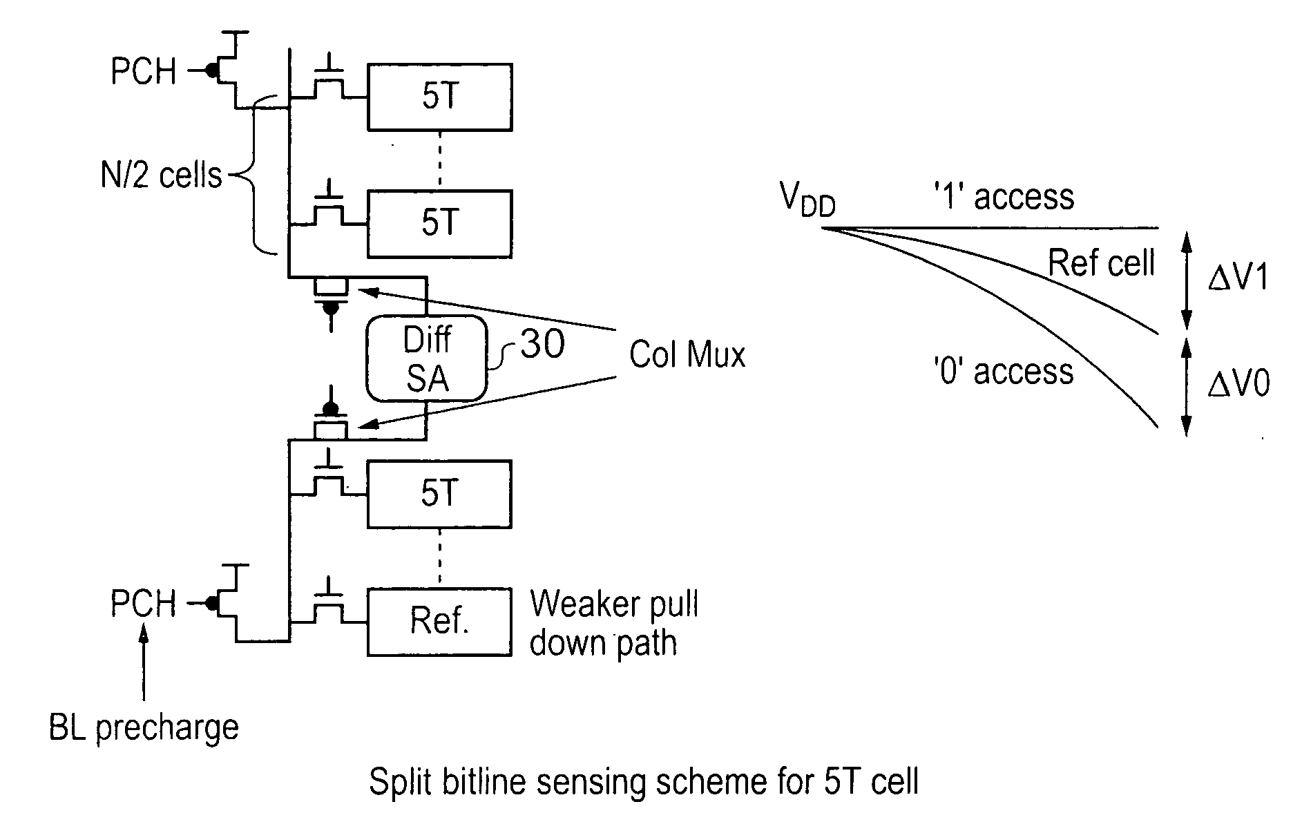
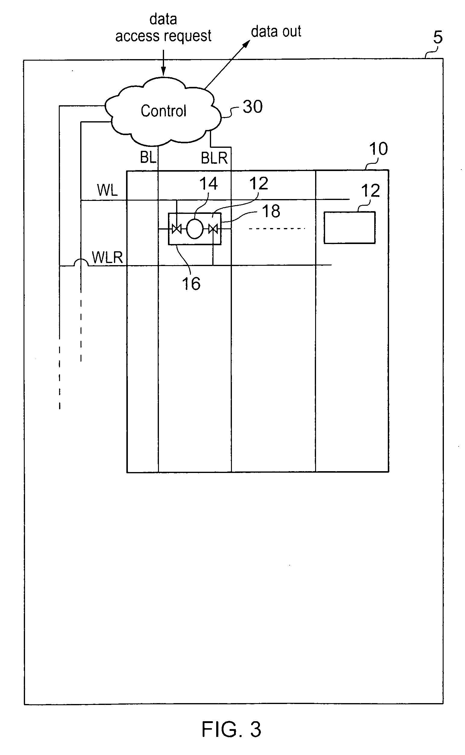
FIG. 3 shows an SRAM memory 5 according to an embodiment of the present invention. Memory 5 comprises an array 10 of storage cells 12, each storing a data value.

These storage cells 12 comprise a storage feedback loop 14, a data access switch 16 and a reset switch 18. The data access switch 16 provides access to the feedback loop from the bit line BL while reset switch 18 provides access to the feedback loop from the reset line BLR. These two switches are controlled by control signals sent along word line WL and reset line WLR. These signals are generated by control circuitry 30 in response to data access requests received from a processor. If the request is a read request then data is output by detecting changes on the data line BL.

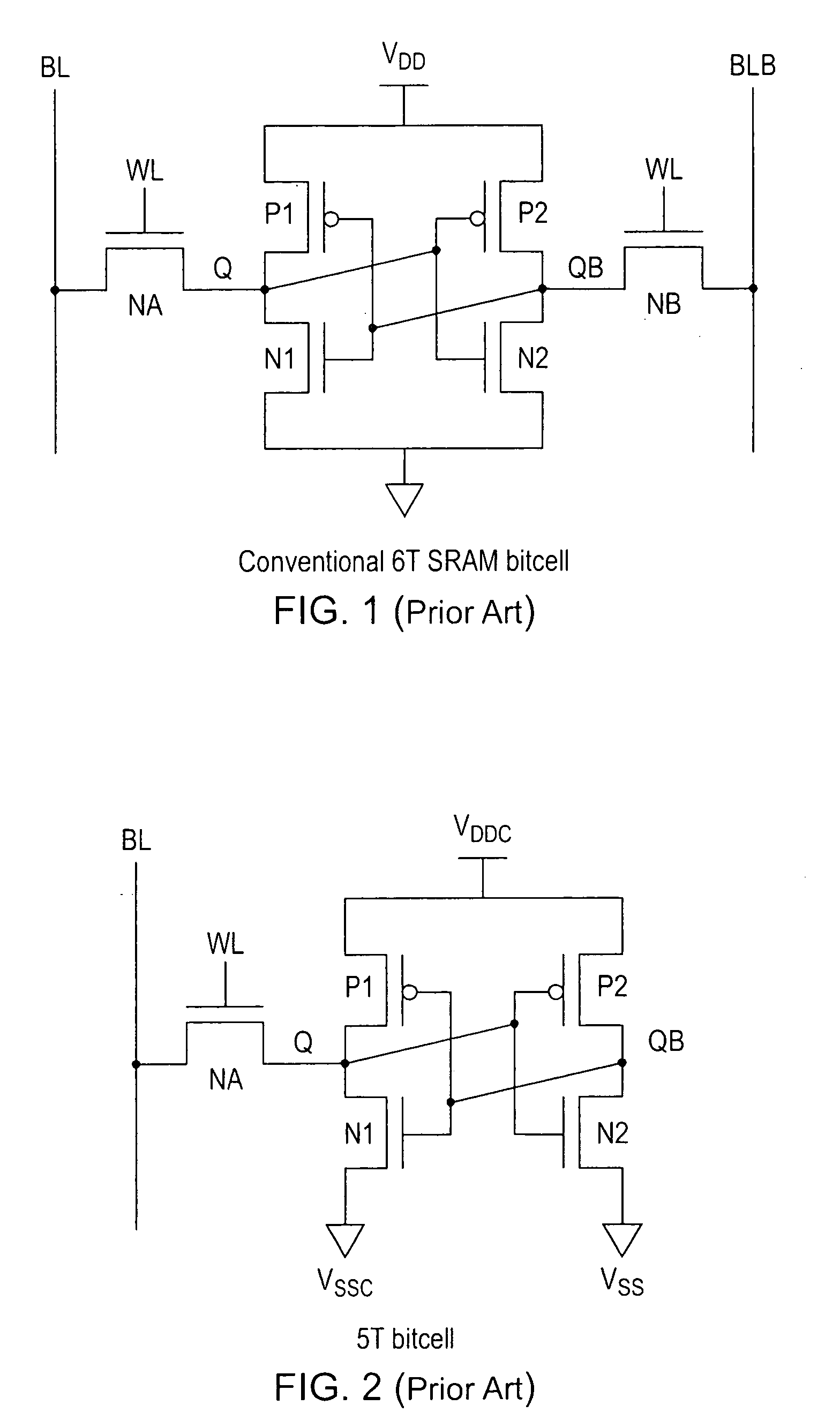
FIG. 4 shows the storage cell 12 in greater detail. In this embodiment, the storage cell is a 6 transistor 6T cell in which the data access switch 16 is a transistor controlled by a signal on the word line WL while the reset switch 18 is a transistor cont...


PUM


Abstract

A static random access memory is disclosed. The SRAM comprises: at least one data line for transferring data to and from the memory and at least one reset line; a plurality of storage cells each being arranged for connection to the at least one data line and the at least one reset line, each storage cell comprising: an asymmetric feedback loop, the feedback loop comprising a first access node for holding a data value when the feedback loop stores the data value and a second access node for holding a complementary version of the data value when the feedback loop stores the data value; an access device for selectively providing a connection between the at least one data line and the first access node; a reset device for selectively providing a connection between the at least one reset line and the second access node; the memory further comprising: data access control circuitry for generating control signals in response to data access requests for independently controlling the access device and the reset device to provide the connections; wherein: the data control circuitry is configured to: generate a data access control signal to trigger the access device to provide the connection between the first access node and the at least one data line in response to a write request to write a predetermined value to the storage cell, and in response to a read request to read a stored value from the storage cell; and generate a reset control signal to trigger the reset device to provide the connection between the at least one reset line and the second access node in response to a write request to write the complementary predetermined value to the storage cell.

Description

BACKGROUND OF THE INVENTION1. Field of the InventionThe field of the invention relates to the field of data storage and in particular, to the storage and access of data in semiconductor memories.2. Description of the Prior ArtThere is a desire to reduce the size and power consumption of a memory. However, as the devices forming a memory and their power consumption reduce, their robustness to corruption tends to decrease. It is becoming increasingly challenging to design robust semiconductor memories such as SRAM that are both small and consume low power.As dimensions scale down the variations in device property due to random dopant fluctuations, line edge roughness etc. increase drastically. Thus, designing a robust SRAM with these smaller dimensions where cells can be read (without read disturb) and written to across all operational voltage ranges turns out to be very difficult.Several different designs for the bitcells forming an SRAM memory have been proposed to improve their rob...

Claims


Application Information

Patent Timeline
IPC IPC(8): G11C7/10G11C7/02G11C11/00
CPCG11C11/419G11C7/02
Inventor CHANDRA, VIKASNALAM, SATYANAND VIJAYPIETRZYK, CEZARYAITKEN, ROBERT CAMPBELL
Owner ARM LTD
Why Eureka
Try Eureka