Method for preparing silicon intercalated monolayer graphene

a monolayer graphene and silicon intercalation technology, applied in the direction of metal/metal-oxide/metal-hydroxide catalysts, cell components, physical/chemical process catalysts, etc., can solve the drawbacks of epitaxial graphene on metal surface, the method of mechanical exfoliation of graphite cannot meet, and the efficiency is low, so as to achieve the effect of sufficient energy

Inactive Publication Date: 2011-04-14
GAO HONG JUN +8
View PDF6 Cites 13 Cited by
  • Summary
  • Abstract
  • Description
  • Claims
  • Application Information

AI Technical Summary

Benefits of technology

[0009]Hence, in a first aspect there is provided a method for preparing the electronic material, large scale high-quality silicon intercalated epitaxial monolayer graphene on metal surface. This method comprises the steps of growing large scale high-quality graphene on metal surface, depositing silicon on the prepared epitaxial graphene and annealing to high temperature to intercalate the silicon to the interface of graphene and metal surface. Depending on the quantity of the silicon deposited on the graphene surface, the numbers of the silicon layers on the interface can be controlled.
[0010]The growth of large scale high-quality graphene on metal surface may result in cleaning the metal surfaces and exposing the metal surfaces to the hydrocarbon gas precursor at high temperature to get the high-quality epitaxial graphene.
[0011]After the preparing of graphene, the silicon is deposited to the graphene surface by the Molecular Beam Epitaxial (MBE) method. The silicon cluster can be monitored to determine the quantity to be intercalated to the interface in the next step. Then the silicon deposited graphene is annealing to high temperature. This process can provide sufficient energy to the silicon atoms to get cross the barrier caused by the continuous graphene to the interface.

Problems solved by technology

The method by mechanical exfoliation from graphite can not satisfy this due to the low efficiency.
This is one of the drawbacks of the epitaxial graphene on metal surface.
Though intercalation of other metal layer to the interface between graphene and substrate to make the freestanding like graphene, the graphene obtained by this method is still on metal surface, which can not be compatible with traditional silicon devices [Phys. Rev. Lett. 101, 157601 (2008);].

Method used


Image

  • Method for preparing silicon intercalated monolayer graphene
  • Method for preparing silicon intercalated monolayer graphene
  • Method for preparing silicon intercalated monolayer graphene

Examples


Embodiment Construction

[0023]The present invention will be described more fully hereinafter with reference to the accompanying drawings, in which some examples of the embodiments of the invention are shown. Indeed, the present invention may be embodied in many different forms and should not be construed as limitation to the embodiments set forth herein, rather, these embodiments are provided by way of example so that this disclosure will satisfy applicable legal requirements. Like numbers refer to like elements throughout.

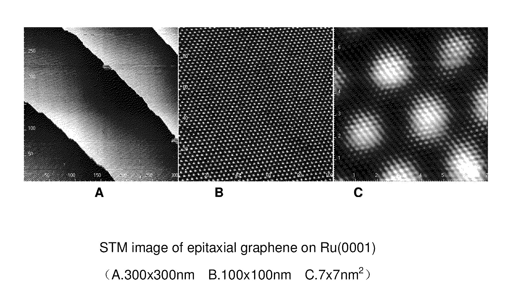
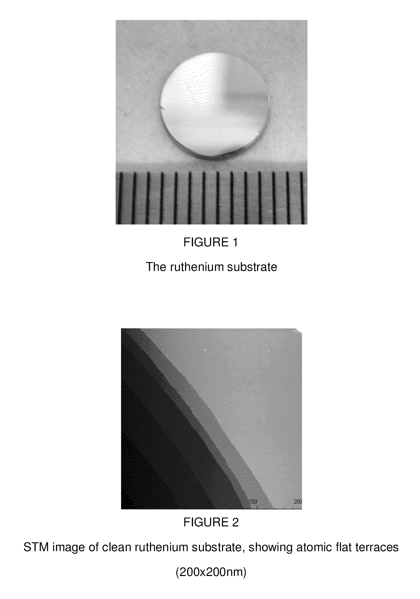
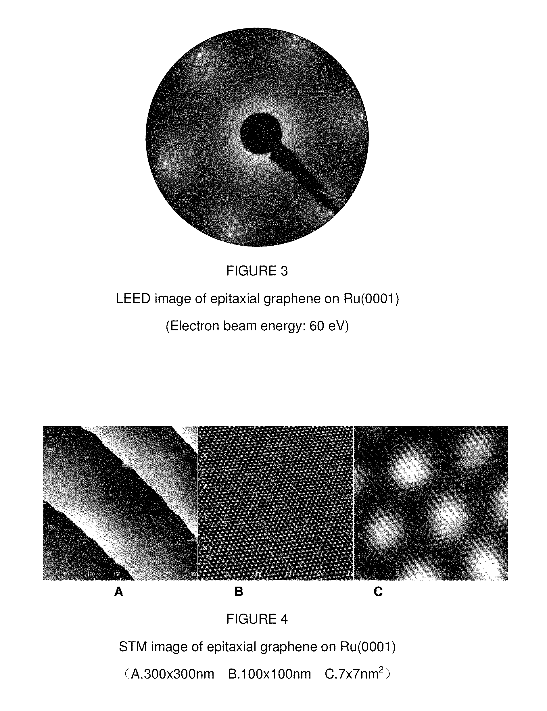
[0024]FIG. 1 shows the photo of the metal surface used to grow graphene. In the present example, the aforementioned Ruthenium orientation 0001 (Ru(0001)) substrate is utilized. The choosing of single crystal is just for checking the quality of graphene by the aforementioned STM easier. The same method is also applicable to polycrystalline metal substrate, as set forth above. FIG. 2 describes the aforementioned clean surface of the Ru(0001) surface, as set forth above. The aforementioned ...


PUM

PropertyMeasurementUnit
pressureaaaaaaaaaa
temperatureaaaaaaaaaa
pressureaaaaaaaaaa

Abstract

A method of preparing the electronic material called silicon intercalated epitaxial monolayer graphene comprises the steps of growing large scale high-quality graphene on metal surface, depositing silicon on the prepared epitaxial graphene and annealing to high temperature to intercalate the silicon to the interface of graphene and metal surface. Depending on the quantity of the silicon deposited on the graphene surface, the numbers of the silicon layers on the interface can be controlled and adjusted.

Description

BACKGROUND OF THE INVENTION[0001]1. Field of the Invention[0002]The present invention relates to a method for preparing the electronic material, silicon intercalated epitaxial monolayer graphene. Specifically, by combining two conventional techniques, large scale high-quality silicon intercalated monolayer graphene was prepared in a controllable way. This approach can have a great potential of application in the future electronic logic devices based on graphene.[0003]2. Description of the Related Art[0004]Since the first piece of monolayer graphene was obtained from highly oriented pyrolytic graphite (HOPG) via mechanical exfoliation method in 2004, it has pushed the upsurge of the investigation on this new two-dimensional materials due to its promising application potential in electronics, information storage materials and catalysis.[0005]Needless to say, for the application in the industry, the large scale high-quality graphene is needed. The method by mechanical exfoliation from ...

Claims


Application Information

Patent Timeline
Patent Type & Authority Applications(United States)
IPC IPC(8): B01J37/025B01J37/08B01J21/18H01L21/322B82Y40/00
CPCB82Y30/00B82Y40/00H01L21/02425H01L21/02433H01M4/583H01L21/0245H01L21/02532H01L21/02694H01M4/366H01L21/02444H01L21/02488H01L21/02527Y02E60/10
Inventor GAO, HONG-JUNPAN, YIGAO, MINMAO, JINHAIHUANG, LIZHOU, HAITAOWANG, YELIANGGUO, HAIMINGDU, SHIXUAN
Owner GAO HONG JUN
Why Eureka
Try Eureka