Light-emiting device chip with micro-lenses and method for fabricating the same

Inactive Publication Date: 2011-04-21
VISERA TECH CO LTD
View PDF7 Cites 16 Cited by
  • Summary
  • Abstract
  • Description
  • Claims
  • Application Information

AI Technical Summary

Problems solved by technology

Advantages of LED chips compared with traditional lamps are lower power consumption and longer lifespan.
In conventional LED chips, the emitted light cannot be effectively extracted from the chip due to the total intern

Method used


Image

  • Light-emiting device chip with micro-lenses and method for fabricating the same
  • Light-emiting device chip with micro-lenses and method for fabricating the same
  • Light-emiting device chip with micro-lenses and method for fabricating the same

Examples


Embodiment Construction

[0016]The following description is of the best-contemplated mode of carrying out the invention. This description is provided for the purpose of illustrating the general principles of the invention and should not be taken in a limiting sense. The scope of the invention is best determined by reference to the appended claims.

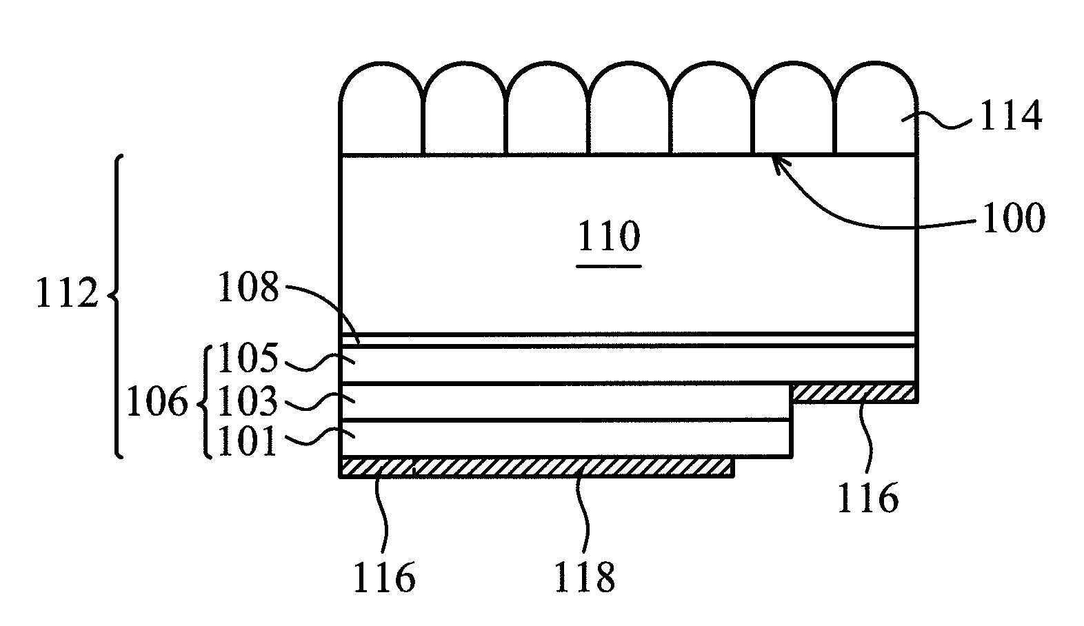
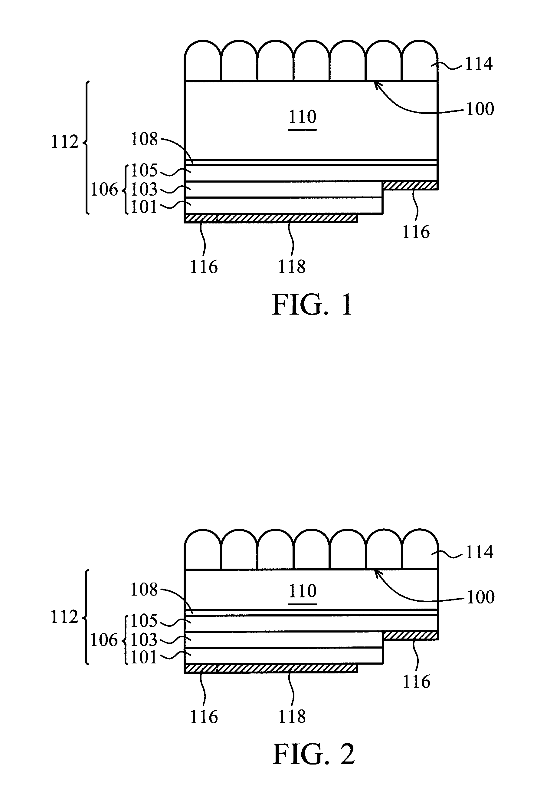
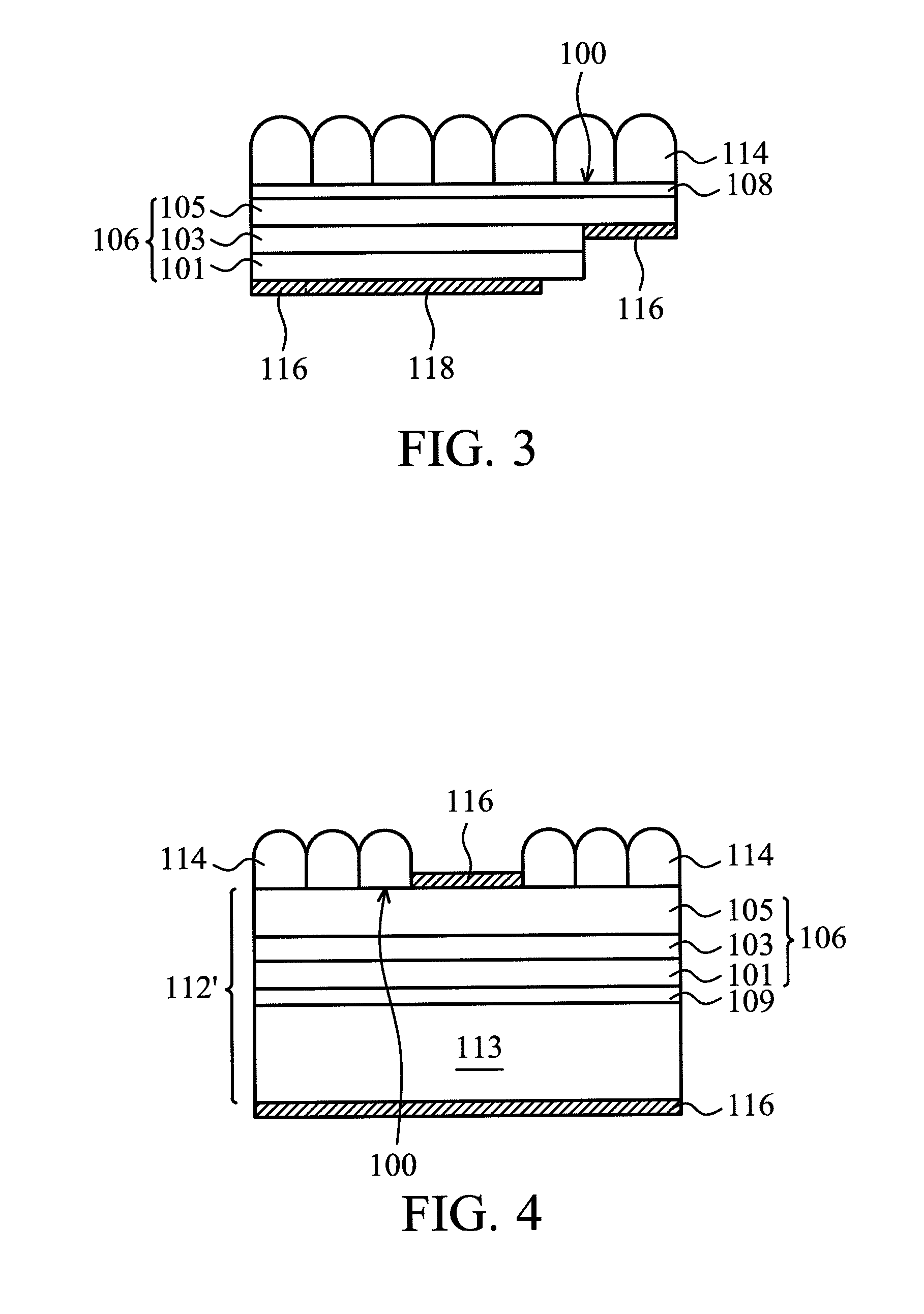
[0017]FIGS. 1 to 4 are cross sections of various exemplary embodiments of a light-emitting device (LED) chip according to the invention. Elements in FIGS. 2 to 4 that are the same as those in FIG. 1 are labeled with the same reference numbers as in FIG. 1 and are not described again for brevity. Referring to FIG. 1, the LED chip can be a red, green, blue, or white LED chip, which comprises a body 112 having a light extraction surface 100, a plurality of micro-lenses 114, and a pair of bond pads 116. In the embodiment, the body may comprise semiconductor layers 106 and a sapphire substrate 110 with a thickness of about 90 μm to 150 μm thereon. The semiconductor laye...


PUM


Abstract

A light-emitting device (LED) chip is disclosed. The LED chip includes a body having a light extraction surface. The body includes semiconductor layers including an n-type region and a p-type region. A plurality of micro-lenses is directly on the light extraction surface of the body. A pair of bond pads is electrically connected to the n-type and p-type regions, respectively. A method for fabricating the LED chip and an LED package with the LED chip are also disclosed.

Description

BACKGROUND OF THE INVENTION[0001]1. Field of the Invention[0002]The invention relates to a light-emitting device (LED) and more particularly to LED chip with micro-lenses and methods for fabricating the same.[0003]2. Description of the Related Art[0004]Light-emitting device (LED) chips (dice) are solid-state light sources and have been known for years. The LED chips are based on the recombination of electron-hole pairs in a pn-junction in a semiconductor material which is forward-biased. Advantages of LED chips compared with traditional lamps are lower power consumption and longer lifespan. To increase an LED chip's reliability and lower its energy consumption, increasing light-emitting efficiency thereof is required.[0005]Light-emitting efficiency is affected by light extraction efficiency of the LED chip. The light extraction efficiency is determined by the structure, the light absorption index and refractive index of LED chips. Accordingly, to further increase the light-emitting ...

Claims


Application Information

Patent Timeline
IPC IPC(8): H01L33/00H01L21/78
CPCH01L33/44H01L33/54H01L2224/13H01L33/58H01L2933/0025
Inventor KUO, WU-CHENGTSENG, CHI-XIANG
Owner VISERA TECH CO LTD
Why Eureka
Try Eureka