

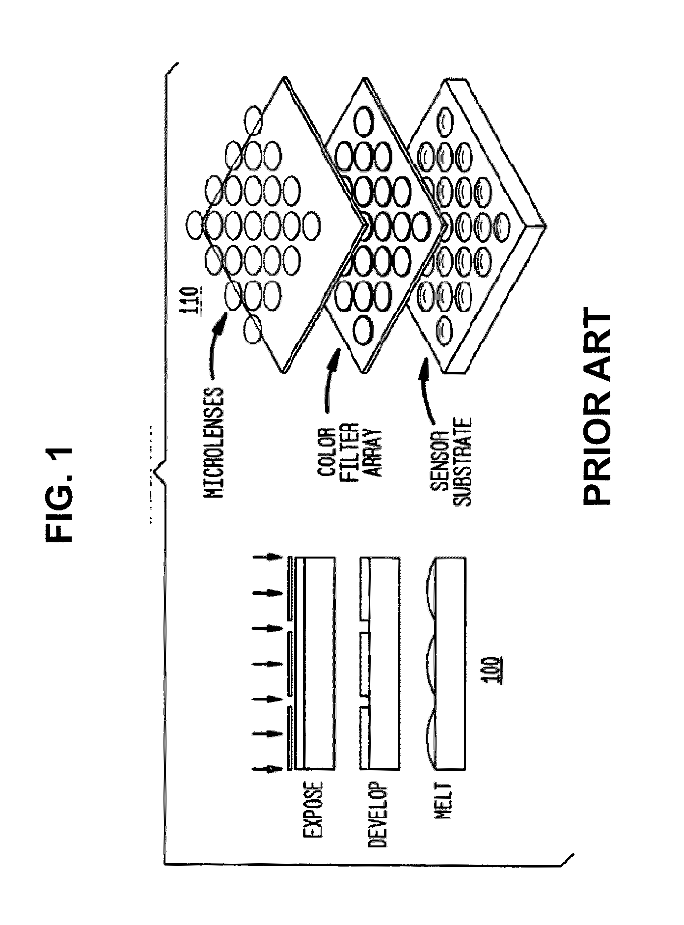
Fabrication of optical filters integrated with injection molded microlenses
a technology of optical filters and microlenses, applied in the field of injection molding of optical components, can solve the problems of high-precision optical components, difficult manufacturing of highly precise optical elements, and difficulty in aligning with led, ccd, cmos or wavelength selective devices, etc., and achieve the effect of reducing the overall cos
- Summary
- Abstract
- Description
- Claims
- Application Information
AI Technical Summary
Benefits of technology
Problems solved by technology
Method used
Image

Examples
Embodiment Construction
[0025]The terminology used herein is for the purpose of describing particular embodiments only and is not intended to be limiting of the invention. As used herein, the singular forms “a”, “an” and “the” are intended to include the plural forms as well, unless the context clearly indicates otherwise. It will be further understood that the terms “comprises” and / or “comprising,” when used in this specification and claims, specify the presence of stated features, integers, steps, operations, elements, and / or components, but do not preclude the presence or addition of one or more other features, integers, steps, operations, elements, components, and / or groups thereof. In the following description, reference is made to the accompanying drawings where like reference numerals refer to like parts throughout the disclosure.
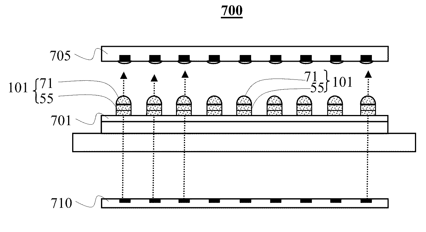
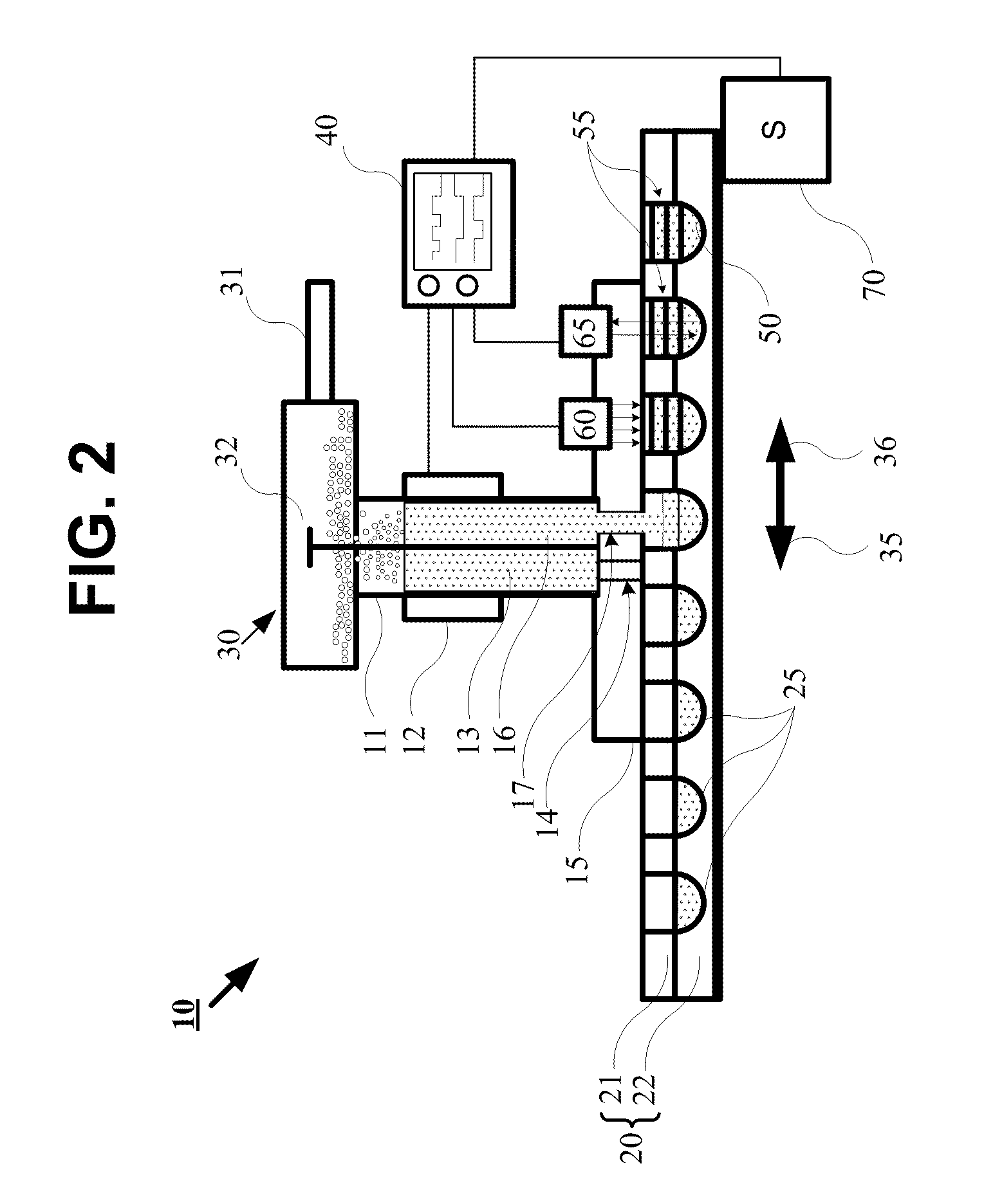
[0026]At least one embodiment of the present invention discloses a system and method for the formation of integrated optical elements, such as spectral filtering devices in...
PUM
| Property | Measurement | Unit |
|---|---|---|
| diameter | aaaaa | aaaaa |
| melting point temperature | aaaaa | aaaaa |
| wavelength range | aaaaa | aaaaa |
Abstract
Description
Claims
Application Information