Device mounting board and semiconductor module

a technology of device mounting and semiconductor module, which is applied in the directions of resist details, semiconductor/solid-state device details, printed circuit aspects, etc., can solve the problems of likely cracks between solder balls and electrode pads, and achieve the effect of improving connection reliability

Inactive Publication Date: 2011-05-05
SANYO ELECTRIC CO LTD
View PDF1 Cites 9 Cited by
  • Summary
  • Abstract
  • Description
  • Claims
  • Application Information

AI Technical Summary

Benefits of technology

[0009]The present invention has been made in view of the foregoing circumstances, and a purpose thereof is to provide a technology by which to improve the connection reliability between electrodes and connection members such as solder balls in a device mounting board.
[0011]By employing this embodiment, the top portion of the electrode portion does not have sharp corners where the stress otherwise tends to be concentrated. Thus, the stress is less likely to be concentrated on the top portion thereof when the bonding members such as solder balls are joined to the electrode portions. As a result, the connection reliability between the electrode portions and the bonding members can be improved when the bonding members are jointed to the electrode portions.
[0016]By employing this embodiment, the wiring layer is electrically connected to the electrode portion at a lower part thereof via the leading portion, and the leading portion is not exposed. As a result, the disconnection of the leading portions is suppressed and therefore the connection reliability between the electrode portions and the connection members such as solder balls can be improved.

Problems solved by technology

In the structure where there is provided a stepped portion in the electrode pad, there is a problem where the stress tends to be concentrated in corners (edges) of the electrode pad and cracks are likely to occur between the solder balls and the electrode pad.

Method used


Image

  • Device mounting board and semiconductor module
  • Device mounting board and semiconductor module
  • Device mounting board and semiconductor module

Examples


first embodiment

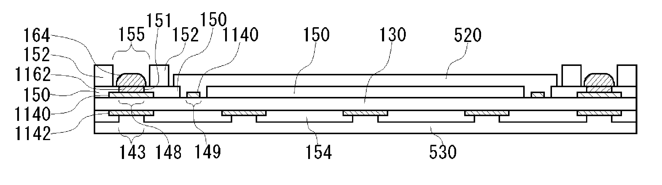
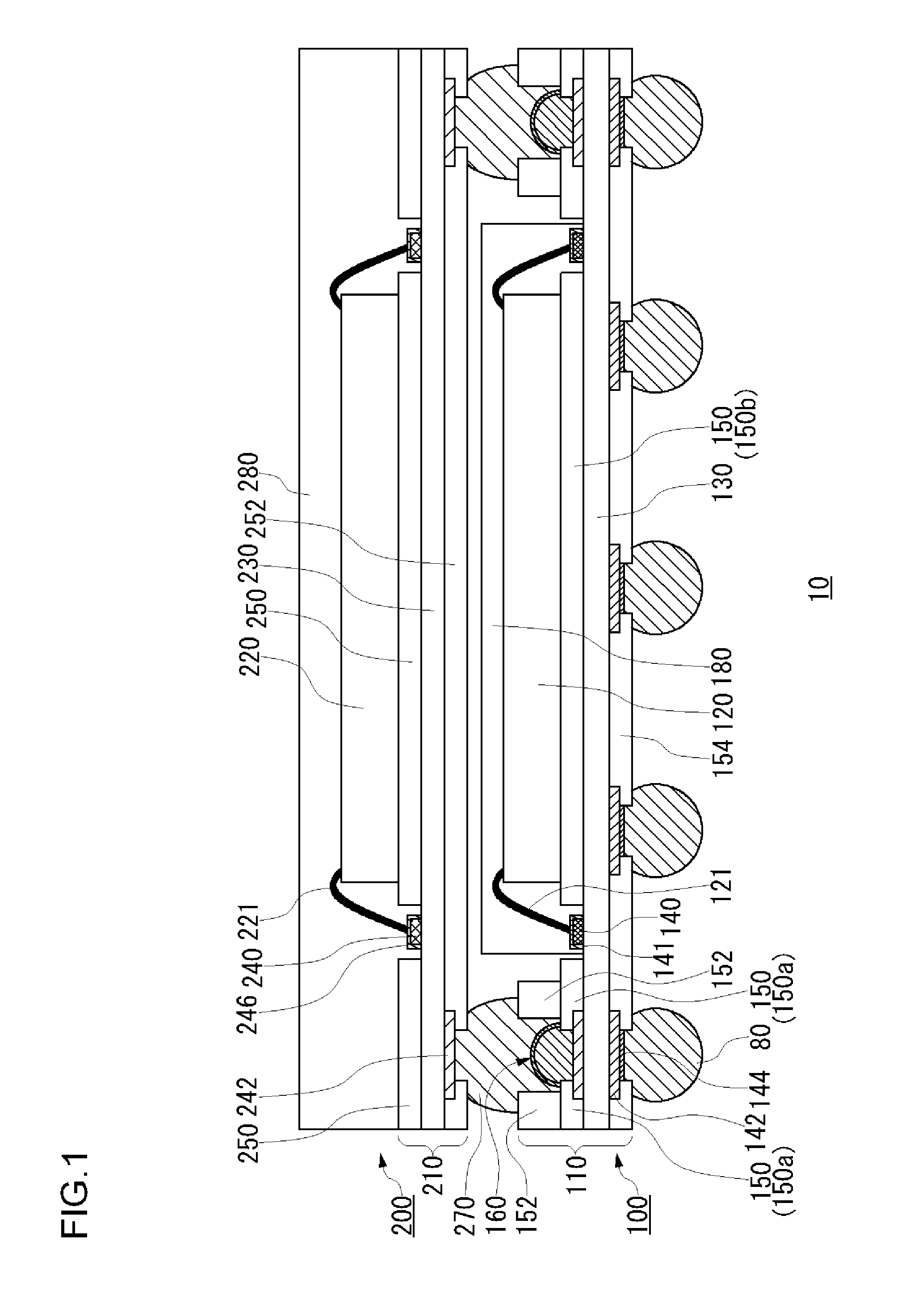
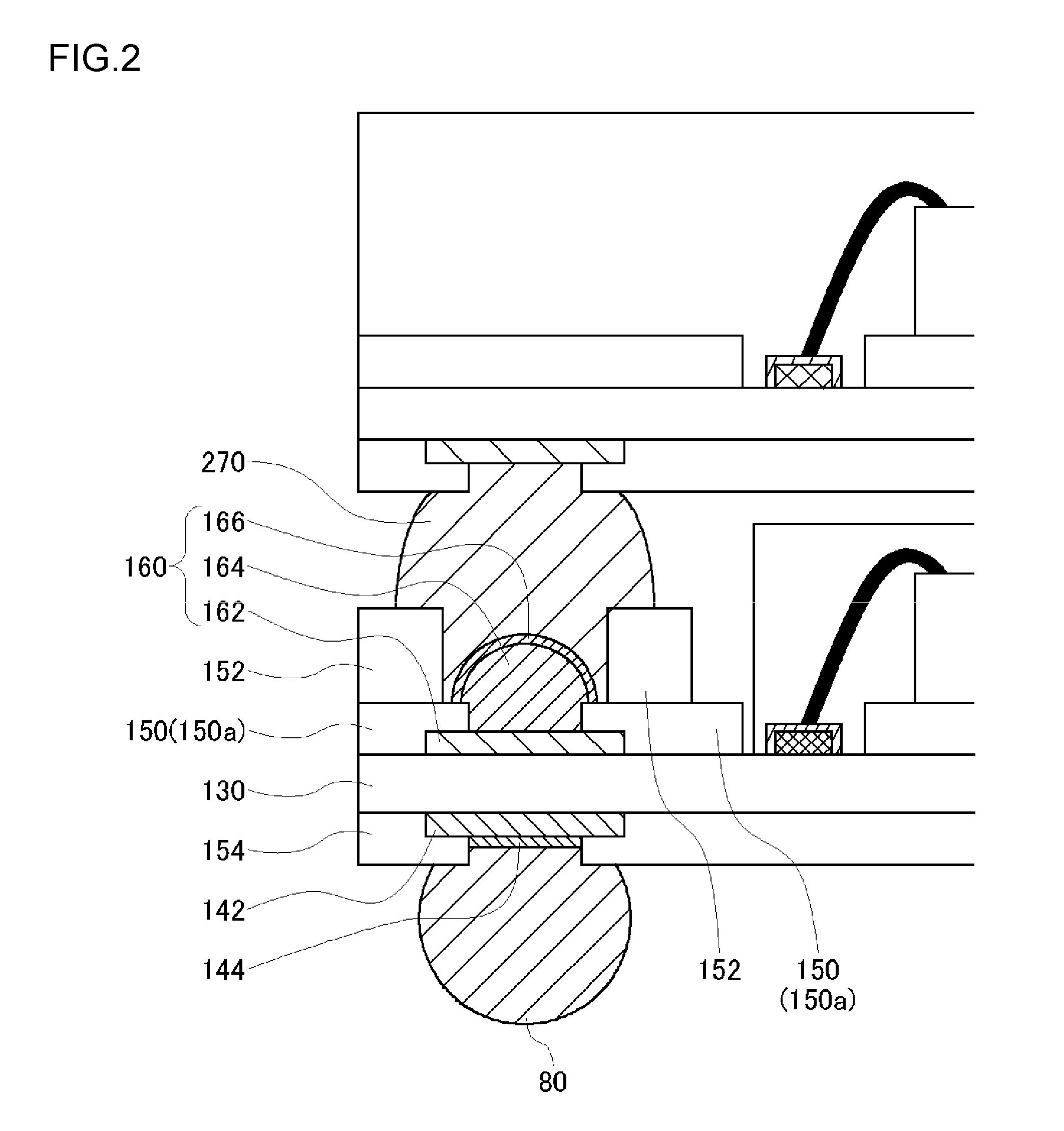
[0039]FIG. 1 is a schematic cross-sectional view showing a structure of a semiconductor device 10 according to a first embodiment of the present invention. FIG. 2 is a partial enlarged view showing a structure of a first electrode portion 160 in the semiconductor device 10 and the periphery of the first electrode portion 160. The semiconductor device 10 has a package-on-package (PoP) structure. That is, the semiconductor device 10 includes a first semiconductor module 100 and a second semiconductor module 200 stacked on top of the first semiconductor module 100.

[0040]The first semiconductor module 100 is structured such that a first semiconductor device (chip) 120 is mounted on a first device mounting board 10.

[0041]The first device mounting board 10 includes an insulating resin layer 130 as a base material, a wiring layer 140 formed on one of main surfaces of the insulating resin layer 130, a third electrode portion 142 formed on the other of main surfaces of the insulating resin l...

second embodiment

[0079]FIG. 6 is a schematic cross-sectional view showing a structure of a semiconductor device according to a second embodiment of the present invention. The basic structure of the semiconductor device according to the second embodiment is similar to that of the first embodiment, except for the structure of the first electrode portion 160. Thus, as for the semiconductor device according to the second embodiment, the repeated description of the same structural components thereof as those of the first embodiment is omitted as appropriate and a description is hereinbelow given centering around the difference therefrom.

[0080]In the semiconductor device 10 according to the second embodiment, the first electrode portion 160 is shaped such that the top portion of the first electrode portion 160 is formed by a curved surface and a plane surface smoothly connected to the curved surface. More specifically, the shape of the top portion of the first electrode portion 160 is domy with an uppermo...

third embodiment

[0082]FIG. 7 is a schematic cross-sectional view showing a structure of a semiconductor device according to a third embodiment of the present invention. The basic structure of the semiconductor device according to the third embodiment is similar to that of the first embodiment, except for the structure of the first electrode portion 160. Thus, as for the semiconductor device according to the third embodiment, the repeated description of the same structural components thereof as those of the first embodiment is omitted as appropriate and a description is hereinbelow given centering around the difference therefrom.

[0083]In the third embodiment, the uppermost part of the top portion of the first electrode portion 160 is positioned higher than the top surface of the second insulating layer 152.

[0084]By employing the semiconductor device 10 according to the third embodiment, at least the following advantageous effect (5) is achieved in addition to the above-described effects.

[0085](5) Th...


PUM


Abstract

A semiconductor device is of a PoP structure such that first electrode portions provided on a first device mounting board constituting a first semiconductor module and second electrode portions provided in a second semiconductor module are joined together by solder balls. A first insulating layer having an opening is provided on one main surface of an insulating resin layer which is a substrate, and an electrode portion, whose top portion protrudes above the top surface of the first insulating layer, is formed in the opening. A second insulating layer is provided on top of the first insulating layer in the periphery of the top portion of the first electrode portion; the second insulting layer is located slightly apart from the top portion of the first electrode portion. The first electrode portion is shaped such that the top portion is formed by a curved surface or formed by a curved surface and a plane surface smoothly connected to the curved surface.

Description

CROSS-REFERENCE TO RELATED APPLICATIONS[0001]This application is based upon and claims the benefit of priority from the prior Japanese Patent Applications No. 2009-251466, filed on Oct. 30, 2009, and Japanese Patent Application No. 2009-272855, filed on Nov. 30, 2009, the entire contents of which are incorporated herein by reference.BACKGROUND OF THE INVENTION[0002]1. Field of the Invention[0003]The present invention relates to a device mounting board used to mount semiconductor devices thereon, a semiconductor module and a mobile apparatus.[0004]2. Description of the Related Art[0005]In recent years, with miniaturization and higher performance in electronic devices, demand has been ever greater for further miniaturization and higher density of semiconductor devices used in the electronic devices. In response to such demand, widely known is a semiconductor module stacking technique such as a 3D packaging technique which is called a package-on-package (PoP) where two or more packages...

Claims


Application Information

Patent Timeline
Patent Type & Authority Applications(United States)
IPC IPC(8): H05K1/11
CPCH01L23/3128H01L23/49811H01L2924/01028H01L2224/32225H01L2224/73265H01L24/48H01L2225/1058H01L2225/1023H05K2203/0588H05K2201/10734H05K2201/10515H05K2201/0367H05K3/368H05K3/3452H01L23/49816H01L24/29H01L25/105H01L2224/45144H01L2224/48091H01L2224/48225H01L2224/48227H01L2224/48228H01L2924/01078H01L2924/01079H01L2924/14H01L2924/15311H01L2924/15331H01L2924/1815H01L2924/19041H05K1/111H05K3/3436H01L2924/00014H01L2924/3512H01L2924/00H01L2924/181H01L24/45H01L2924/00012H01L2224/45015H01L2924/207
Inventor NAGAMATSU, MASAYUKISHIBATA, KIYOSHIHAYASHI, TAKANORI
Owner SANYO ELECTRIC CO LTD
Why Eureka
Try Eureka