

Hybrid bonding interface for 3-dimensional chip integration
a technology of hybrid bonding and chip integration, applied in the direction of electrical equipment, semiconductor devices, semiconductor/solid-state device details, etc., can solve the problems of reliability problems in the bonded structure, electrical shorts, and the resistance material of the two substrates does not provide significant adhesion strength between the two substrates
- Summary
- Abstract
- Description
- Claims
- Application Information
AI Technical Summary
Problems solved by technology
Method used
Image

Examples
Embodiment Construction
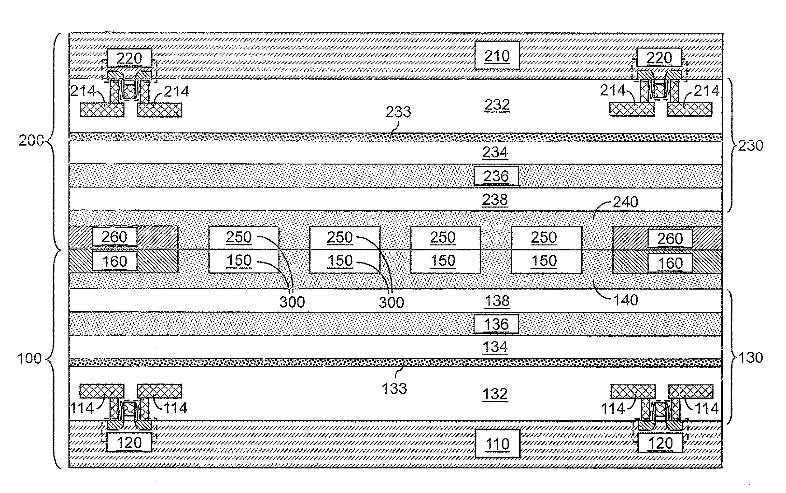
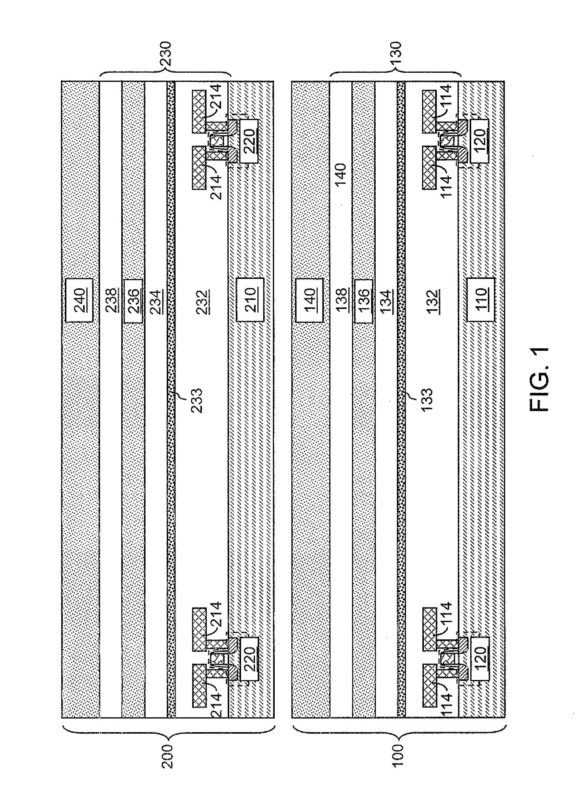
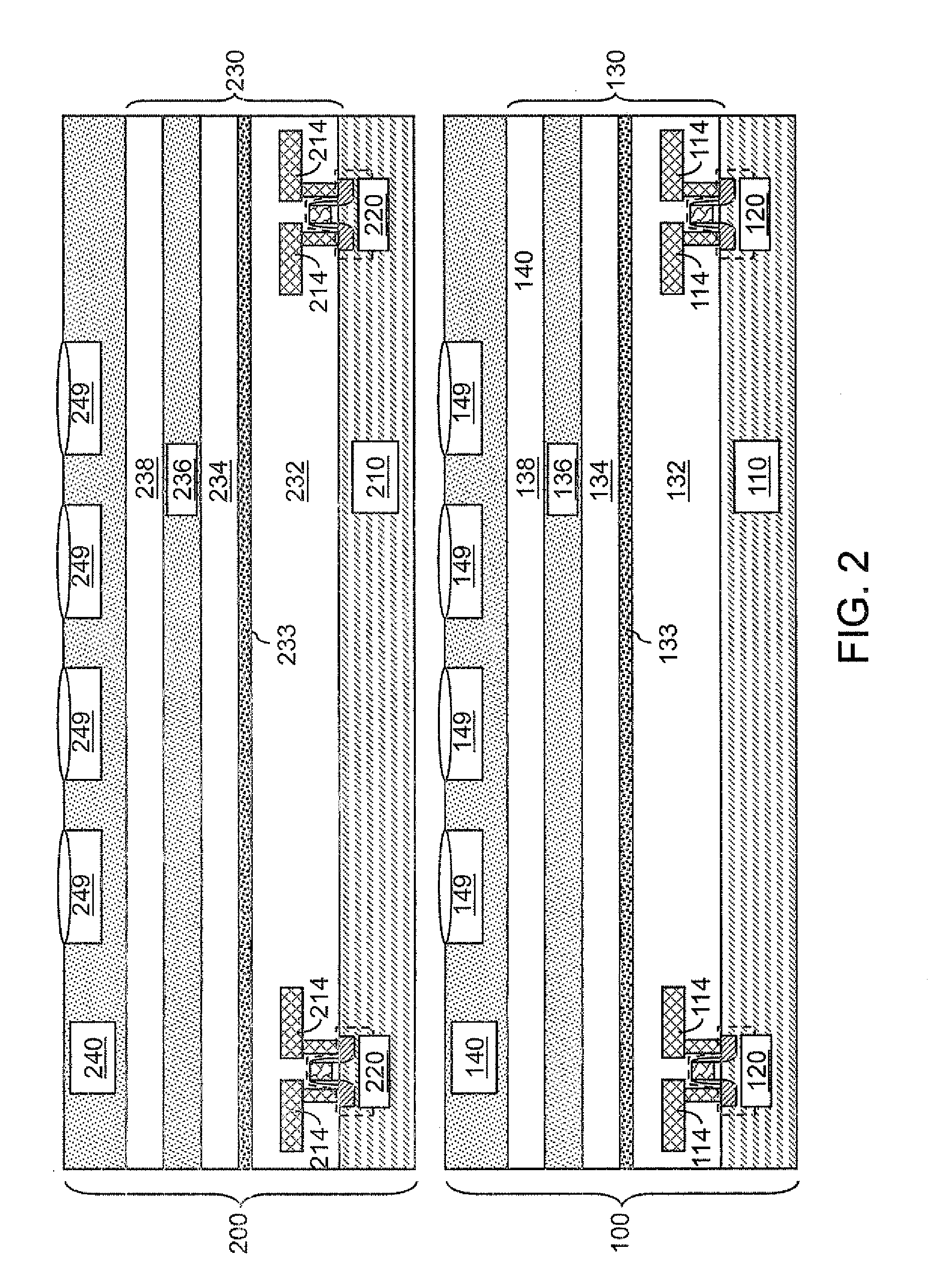
As stated above, the present invention relates to a bonded structure that provides high adhesion strength and containment of interfacial impurity diffusion and methods of manufacturing the same, which are now described in detail with accompanying figures. The drawings are not necessarily drawn to scale.
As used herein, a “bonding” of a first element and a second element is a state or process in which the first element is attached to the second element by adhesion strength generated at an atomic or molecular level at an interface between the first element and the second element.
As used herein, a “bondable dielectric material” is a dielectric material of which two portions can be bonded to provide adhesion strength therebetween under conditions known in the art. For example, silicon oxide is a bondable dielectric material of which two portions can be bonded to provide adhesion strength therebetween under conditions employed for substrate bonding known in the semiconductor industry.
As u...
PUM
| Property | Measurement | Unit |
|---|---|---|
| thicknesses | aaaaa | aaaaa |
| thicknesses | aaaaa | aaaaa |
| thicknesses | aaaaa | aaaaa |
Abstract
Description
Claims
Application Information