Solid-state imaging element and camera system

a camera system and imaging element technology, applied in the field of solid-state imaging elements and camera systems, can solve the problems of large number of dummy pixels, high cost and power consumption, and achieve the effect of suppressing image noise and reducing the number of times

Inactive Publication Date: 2011-05-05
SONY SEMICON SOLUTIONS CORP
View PDF8 Cites 14 Cited by
  • Summary
  • Abstract
  • Description
  • Claims
  • Application Information

AI Technical Summary

Benefits of technology

[0039]The present invention contributes to significantly reduced number of times a dummy shutter is operated which is used to suppress image noise caused by a shutter level difference during a frame period.

Problems solved by technology

Therefore, as described in Patent Document 2, if as many dummy pixels are provided as for two frames of shuttered rows, this leads to a large number of dummy pixels, thereby resulting in higher cost and higher power consumption.

Method used


Image

  • Solid-state imaging element and camera system
  • Solid-state imaging element and camera system
  • Solid-state imaging element and camera system

Examples


first embodiment

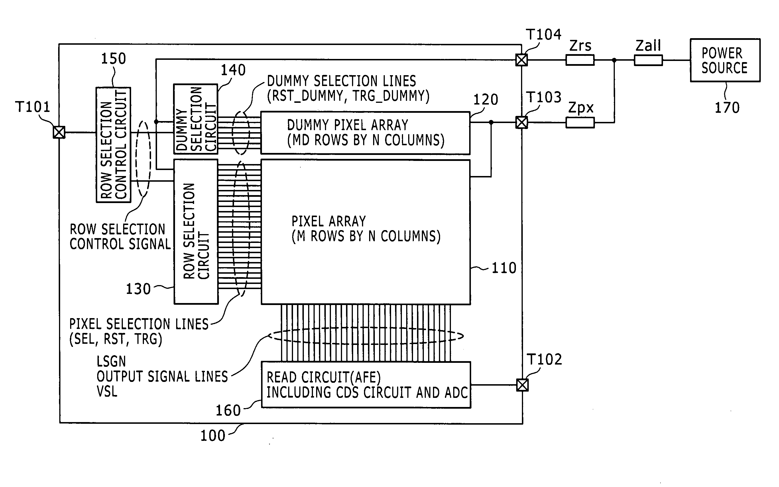
[0054]FIG. 4 is a diagram illustrating a configuration example of a CMOS image sensor (solid-state imaging element) according to an embodiment of the present invention.

[0055]A CMOS image sensor 100 includes a pixel array section 110, dummy pixel array section 120, row selection circuit 130, dummy selection circuit 140, row selection control circuit 150 and read circuit (AFE) 160.

[0056]The row selection circuit 130, dummy selection circuit 140 and row selection control circuit 150 make up pixel drive sections.

[0057]The CMOS image sensor 100 further includes an input terminal T101 for an operation mode selection signal MDS, a data output terminal 102, pixel power terminal T103 and row selection circuit power terminal T104.

[0058]The pixel array section 110, dummy pixel array section 120, row selection circuit 130 and dummy selection circuit 140 of the CMOS image sensor 100 are supplied with power from an external power source 170 via the pixel power terminal T103 and row selection circ...

second embodiment

[0155]FIG. 10 is a diagram illustrating a configuration example of a camera system to which a solid-state imaging element according to a second embodiment is applied.

[0156]As illustrated in FIG. 10, a camera system 200 includes an imaging device 210 to which the CMOS image sensor (solid-state imaging element) 100 according to the present embodiment is applicable.

[0157]The camera system 200 further includes an optics adapted to guide incident light into the pixel region of the imaging device 210 such as a lens 220 adapted to form an image of incident light (image light) on the imaging surface.

[0158]The camera system 200 still further includes a driver (DRV) 230 and signal processor (PRC) 240. The driver 230 drives the imaging device 210. The signal processor 240 processes a signal output from the imaging device 210.

[0159]The driver 230 includes a timing generator (not shown) to drive the imaging device 210 with given timing signals. The timing generator generates a variety of timing ...


PUM


Abstract

A solid-state imaging element includes: a pixel section having a plurality of pixels arranged in a matrix form, each of the pixels converting an optical signal into an electric signal and storing the electric signal according to exposure time; a dummy pixel section having dummy pixels arranged in a matrix form; and pixel drive sections adapted to control the pixel operations in such a manner as to operate an electronic shutter on and read the pixel section and dummy pixel section, wherein when an electronic rolling shutter is operated in which the pixels are shuttered row by row, the pixel drive sections judge whether the current and next frames are shuttered concurrently and in parallel so as to determine in which horizontal read period the dummy pixel section is to be shuttered.

Description

BACKGROUND OF THE INVENTION[0001]1. Field of the Invention[0002]The present invention relates to a solid-state imaging element and camera system for performing shuttering based on rolling shutter.[0003]2. Description of the Related Art[0004]Global shutter and rolling shutter (focal plane shutter) are known as types of electronic shutter for use in image sensors having photoelectric conversion elements arranged in a matrix form.[0005]Global shutter is a type of electronic shutter that operates on all the pixels at the same time, whereas rolling shutter is a type of electronic shutter that operates on the pixels row by row.[0006]In many cases, the pixels are read row by row with both global shutter and rolling shutter. With rolling shutter, the row on which an electronic rolling shutter operates and that which is read are shifted over time.[0007]FIG. 1 is a diagram illustrating, for convenience, shuttering and reading in rolling shutter.[0008]In FIG. 1, the horizontal axis represents ...

Claims


Application Information

Patent Timeline
Patent Type & Authority Applications(United States)
IPC IPC(8): H04N5/228H04N5/335
CPCH04N5/3456H04N5/347H04N5/2353H04N5/3591H04N5/3745H04N5/3532H04N25/445H04N25/46H04N25/531H04N25/621H04N25/77H04N23/73
Inventor EBIHARA, HIROAKI
Owner SONY SEMICON SOLUTIONS CORP
Why Eureka
Try Eureka