Method of Forming Metal Interconnect Structures in Ultra Low-K Dielectrics

a technology of ultra-low-k dielectrics and metal interconnects, which is applied in the direction of semiconductor/solid-state device manufacturing, basic electric elements, electric apparatus, etc., can solve the problems of poor electromigration lifetime of wide-line interconnects, fangs are not appropriately covered with liner, and the overall speed of operation of these advanced chips is beginning to be limited

Active Publication Date: 2011-05-19
GLOBALFOUNDRIES US INC
View PDF3 Cites 376 Cited by
  • Summary
  • Abstract
  • Description
  • Claims
  • Application Information

AI Technical Summary

Problems solved by technology

With the progress in the transistor device technology leading to the present ultra large scale integration, the overall speed of operation of these advanced chips are beginning to be limited by the signal propagation delay in the interconnection wires between the individual devices on the chips.
However, the reliability of metal interconnects in porous ultra low-k dielectrics is a critical concern.
In particular, the electromigration lifetime of wide-line interconnects is poor due to a lack of a liner contact between the landing via and the liner in the underlying line.
Since the porous dielectric is prone to severe erosion during etch-back step needed for via embedment within the underlying line, localized “fangs” or deep and sharp trenches are formed at the bottom of the line.
Because of the severe topography, these fangs are not appropriately covered with the liner.
As a result, in view of a voltage bias, the metal can readily leak out through the exposed area causing time-dependent dielectric breakdown (TDDB) leakage failure as well as time-zero leakage.
At present, there are no known solutions to this problem.

Method used


Image

  • Method of Forming Metal Interconnect Structures in Ultra Low-K Dielectrics
  • Method of Forming Metal Interconnect Structures in Ultra Low-K Dielectrics
  • Method of Forming Metal Interconnect Structures in Ultra Low-K Dielectrics

Examples


Embodiment Construction

[0021]In the following description, numerous specific details are set forth, such as particular structures, components, materials, dimensions, processing steps and techniques, in order to provide a thorough understanding of the present disclosure. However, it will be appreciated by one skilled in the art that the invention may be practiced without these specific details. In other instances, well-known structures or processing steps have not been described in detail to avoid obscuring the invention. Thus, the materials and dimensions described herein are employed to illustrate the invention in one application and should not be construed as limiting.

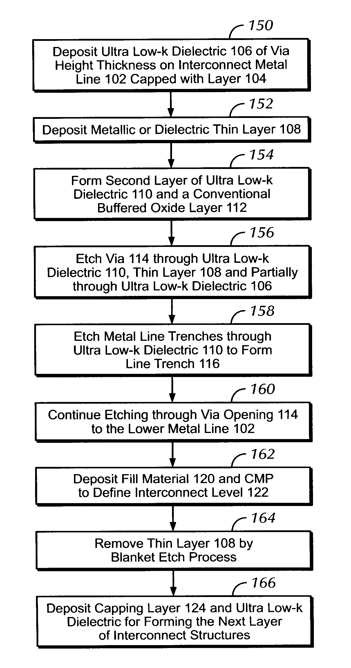
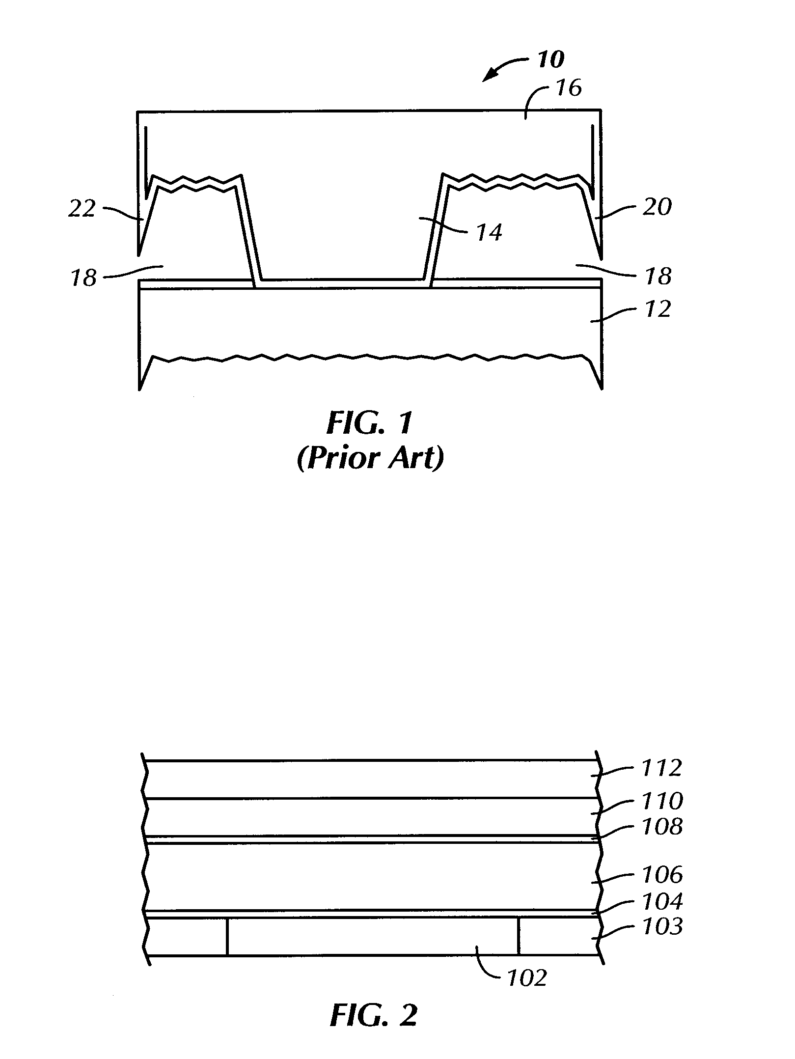
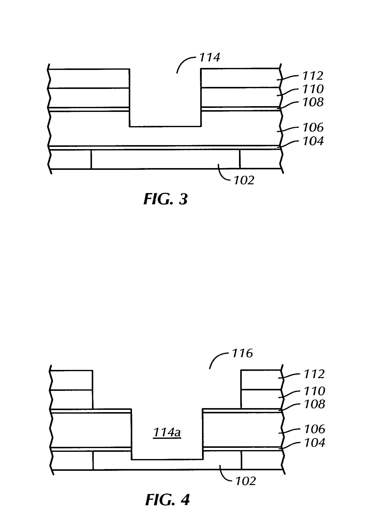
[0022]Referring now to the drawing figures, wherein like references numerals identify identical or corresponding elements, an embodiment of the presently disclosed structure and method of forming metal interconnect structures in ultra low-k dielectrics, will be disclosed in detail. In particular, a new interconnect process is described, wh...


PUM

PropertyMeasurementUnit
thicknessaaaaaaaaaa
thicknessaaaaaaaaaa
dielectric constantaaaaaaaaaa

Abstract

A metal interconnect structure in ultra low-k dielectrics is described having a capped interconnect layer; an interconnect feature with a contact via and a contact line formed in a dielectric layer, where the via is partially embedded into the interconnect layer; and a thin film formed on the dielectric layer and separating the dielectric layer from the contact line. A method of fabricating the interconnect structure is also described and includes forming a first dielectric on a capped interconnect element; forming a thin film over the first dielectric; forming a second dielectric on the thin film; forming a via opening on the second dielectric, the thin film and extending into the first dielectric; forming a line trench on a portion of the second dielectric; and filling the via opening and the line trench with a conductive material for forming a contact via and a contact line, where the contact via is partially embedded in the interconnect element.

Description

CROSS-CORRELATION WITH RELATED PATENTS[0001]The present application is a Divisional of U.S. patent application Ser. No. 12 / 351,272, filed Jan. 9, 2009, entitled “Structure and Method of Forming Metal Interconnect Structures in Ultra Low-K Dielectrics”.BACKGROUND OF THE INVENTION[0002]1. Technical Field[0003]The present disclosure relates generally to interconnect structures formed in semiconductor devices. In particular, the present disclosure relates to a structure and methods of forming metal interconnect structures in porous ultra low-k dielectric.[0004]2. Description of Related Art[0005]Integrated circuit chips typically include two or more levels of conductive lines which are vertically spaced apart and separated by intermediate insulating layers. Interconnections are formed between the levels of conductive lines in the chip for providing high wiring density and good thermal performance. The interconnections are formed by means of lines and vias which are etched through the ins...

Claims


Application Information

Patent Timeline
Patent Type & Authority Applications(United States)
IPC IPC(8): H01L21/768
CPCH01L21/76805H01L21/76807H01L21/76885H01L21/76829H01L21/76841H01L21/76813
Inventor AGARWALA, BIRENDRANGUYEN, DURATHORE, HAZARA
Owner GLOBALFOUNDRIES US INC
Why Eureka
Try Eureka