Supercharge Your Innovation With Domain-Expert AI Agents!

Manufacturing method for thin film type light absorbing layer, manufacturing method for thin film solar cell using thereof and thin film solar cell

a manufacturing method and technology of light absorbing layer, applied in the field of thin film solar cells, can solve the problems of difficult to accurately control the evaporation temperature or evaporation speed, difficult to control the composition ratio of each element of the cigs, and difficult to accurately control the composition of the cigs light absorbing layer. , to achieve the effect of reducing the amount of time, improving process efficiency and low cos

Inactive Publication Date: 2011-05-26
ELECTRONICS & TELECOMM RES INST
View PDF17 Cites 10 Cited by
  • Summary
  • Abstract
  • Description
  • Claims
  • Application Information

AI Technical Summary

Benefits of technology

[0012]Therefore, it is an object of the present invention to provide a manufacturing method for a thin film type light absorbing layer that can rapidly and simply manufacture a high-quality CIGS light absorbing layer.
[0025]According to the manufacturing method for a thin film type light absorbing layer, the manufacturing method for a thin film solar cell using thereof, and a thin film solar cell, the light absorbing layer is formed by a thermal evaporation deposition method using the CIGS crystal powder, thereby making it possible to form a high-quality CIGS thin film type light absorbing layer.
[0026]In addition, the CIGS crystal powder are simultaneously evaporated, thereby making it possible to reduce the amount of time in the manufacturing process of the thin film type light absorbing layer, increase the process efficiency, and manufacture the high-quality CIGS thin film type light absorbing layer and CIGS thin film solar cell at low cost.

Problems solved by technology

However, when the light absorbing layer is formed by the vaporizing deposition method according to the related art, it is difficult to accurately control an evaporation temperature or an evaporation speed due to having different vaporizing temperatures of each evaporation material and it is difficult to control a composition of the CIGS light absorbing layer due to a phenomenon of when the evaporation materials bounce from an evaporation source.
In addition, when the light absorbing layer is formed by the sputtering deposition method according to the related art, it is difficult to control a composition ratio of each element of the CIGS and further, the sputtering using the anion of selenium impacts the light absorbing layer such that the light absorbing layer has many defects.
Therefore, the manufacturing method for a light absorbing layer in the related art requires a long manufacturing process and complication process, thereby making it difficult to control the composition.

Method used


Image

  • Manufacturing method for thin film type light absorbing layer, manufacturing method for thin film solar cell using thereof and thin film solar cell
  • Manufacturing method for thin film type light absorbing layer, manufacturing method for thin film solar cell using thereof and thin film solar cell
  • Manufacturing method for thin film type light absorbing layer, manufacturing method for thin film solar cell using thereof and thin film solar cell

Examples


Embodiment Construction

[0037]In order to fully understand the benefits in the operation of the present invention and objects to be achieved by exemplary embodiments of the present invention, the accompanying drawings illustrating the exemplary embodiments of the present invention and the contents described in the accompanying drawings should be referred.

[0038]Hereinafter, the exemplary embodiment of the present invention will be described in detail with reference to the accompanying drawings to help understand the present invention. Like reference numerals proposed in each drawing denote like components.

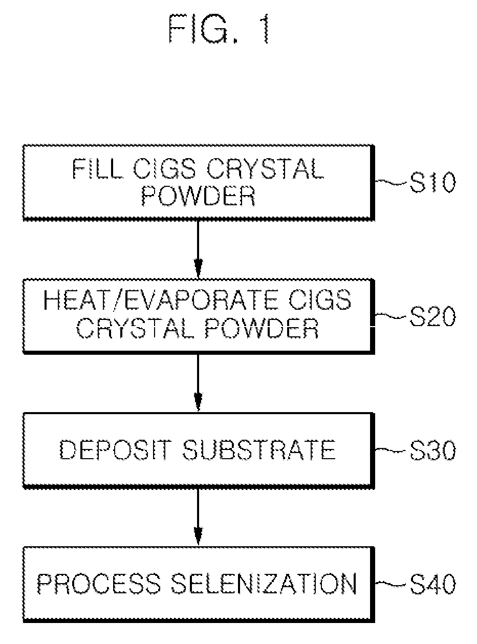
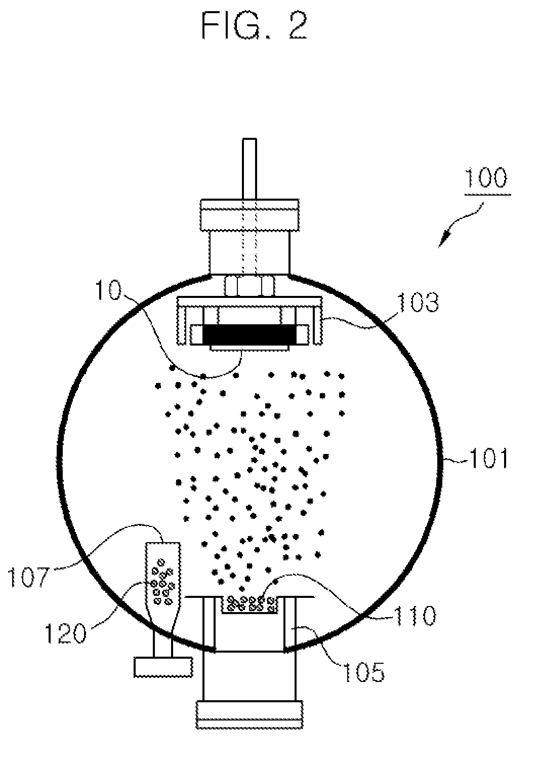
[0039]FIG. 1 is a process flow chart that forms a thin film type light absorbing layer of a thin film solar cell according to one embodiment of the present invention and FIG. 2 is a schematic configuration diagram of an apparatus for forming a thin film type light absorbing layer.

[0040]Referring to FIGS. 1 and 2, an apparatus 100 for manufacturing a thin film type light absorbing layer may include a chambe...


PUM


Abstract

Disclosed is a manufacturing method for a thin film type light absorbing layer of a solar cell. The manufacturing method for a light absorbing layer includes: filling CIGS crystal powder in an evaporation source of a chamber; simultaneously evaporating the CIGS crystal powder; and depositing the evaporated CIGS crystal powder on a substrate to form a CIGS thin film.

Description

RELATED APPLICATIONS[0001]The present application claims priority to Korean Patent Application Serial Number 10-2009-0112414, filed on Nov. 20, 2009, the entirety of which is hereby incorporated by reference.BACKGROUND OF THE INVENTION[0002]1. Field of the Invention[0003]The embodiment relates to a thin film solar cell, and more specifically, to a manufacturing method for a thin film type light absorbing layer formed by CIGS crystal powder, a manufacturing method for a thin film solar cell using thereof, and a thin film solar cell manufactured by the manufacturing method.[0004]2. Description of the Related Art[0005]A solar cell technology has recently been interested as an eco-friendly new renewable energy technology, specifically, as an energy source for commercial power production and portable or mobile electronic devices.[0006]A solar cell is provided with a light absorbing layer for absorbing light, wherein the light absorbing layer is manufactured in a thin film type.[0007]The ...

Claims


Application Information

Patent Timeline
IPC IPC(8): H01L31/032H01L31/18
CPCY02E10/541H01L21/02422H01L21/02491H01L31/0326H01L21/02631H01L31/0749H01L21/02568Y02P70/50H01L31/0445
Inventor SUH, JEONGDAESONG, KIBONGHAM, CHANGWOOCHUNG, MYUNGAESOHN, SUNGWON
Owner ELECTRONICS & TELECOMM RES INST
Features
  • R&D
  • Intellectual Property
  • Life Sciences
  • Materials
  • Tech Scout
  • Unparalleled Data Quality
  • Higher Quality Content
  • 60% Fewer Hallucinations
Learn More