Controlling voltage levels applied to access devices when accessing storage cells in a memory

a technology of access devices and voltage levels, applied in the field of data storage, can solve the problems of increasing the size of devices and power consumption, and the difficulty of designing robust semiconductor memories such as srams, and the design of robust srams where cells can be read (without read disturb) and written to across all operational voltage ranges, and achieves the effect of easy control of the voltage level of access devices

Active Publication Date: 2011-05-26
ARM LTD
View PDF3 Cites 13 Cited by
  • Summary
  • Abstract
  • Description
  • Claims
  • Application Information

AI Technical Summary

Benefits of technology

[0011]The present invention recognises that accessing data within a storage cell via access devices is not always straightforward and that it may be advantageous to change the voltage level supplied to an access device of the storage cell to aid the data access. The present invention provides access control circuitry that has a capacitor and switching circuitry, the switching circuitry being used to connect the capacitor to the access control line that has been selected by the access request. This allows the access control circuitry to control more than one access control line by simply connecting the capacitor to the appropriate line. This means that rather than needing individual access control circuits for each access control line, one circuit can control multiple lines. This provides a significant saving on area. Furthermore, the use of a capacitor to change the voltage value provides the system with great flexibility allowing the voltage level to be amended as is required for the particular circumstance.
[0037]Even when inhibited from changing the voltage level on the access control lines, the access control circuitry can have a positive influence on the memory by charging the capacitor and coupling it to the supply voltage so that it acts as a decoupling capacitor and helps maintain the stability of the supply voltage without adding any loading to the word line.

Problems solved by technology

With ever increasing demands to reduce both the size of devices and their power consumption, it is becoming increasingly challenging to design robust semiconductor memories such as SRAM.
Thus, designing a robust SRAM where cells can be read (without read disturb) and written to across all operational voltage ranges turns out to be very difficult.
Reducing the voltage at which the SRAM cells can be read and written to successfully is not easy and in particular as the voltage scales down it becomes increasingly difficult to write to the cells.
A drawback of this scheme is that there is a significant area overhead resulting from having one extra transistor per word line and also this transistor adds an additional delay to the turning off of the pass gate.
The pass gate allows access to the storage cell, and this extra delay results in some charge leakage and therefore decreases the efficiency of the scheme.
In addition to the above drawbacks, such schemes as this only address the write-ability problems and not the problems associated with read disturb where an increased voltage on the word line makes it more likely that cells may be unintentionally corrupted.

Method used


Image

  • Controlling voltage levels applied to access devices when accessing storage cells in a memory
  • Controlling voltage levels applied to access devices when accessing storage cells in a memory
  • Controlling voltage levels applied to access devices when accessing storage cells in a memory

Examples


Embodiment Construction

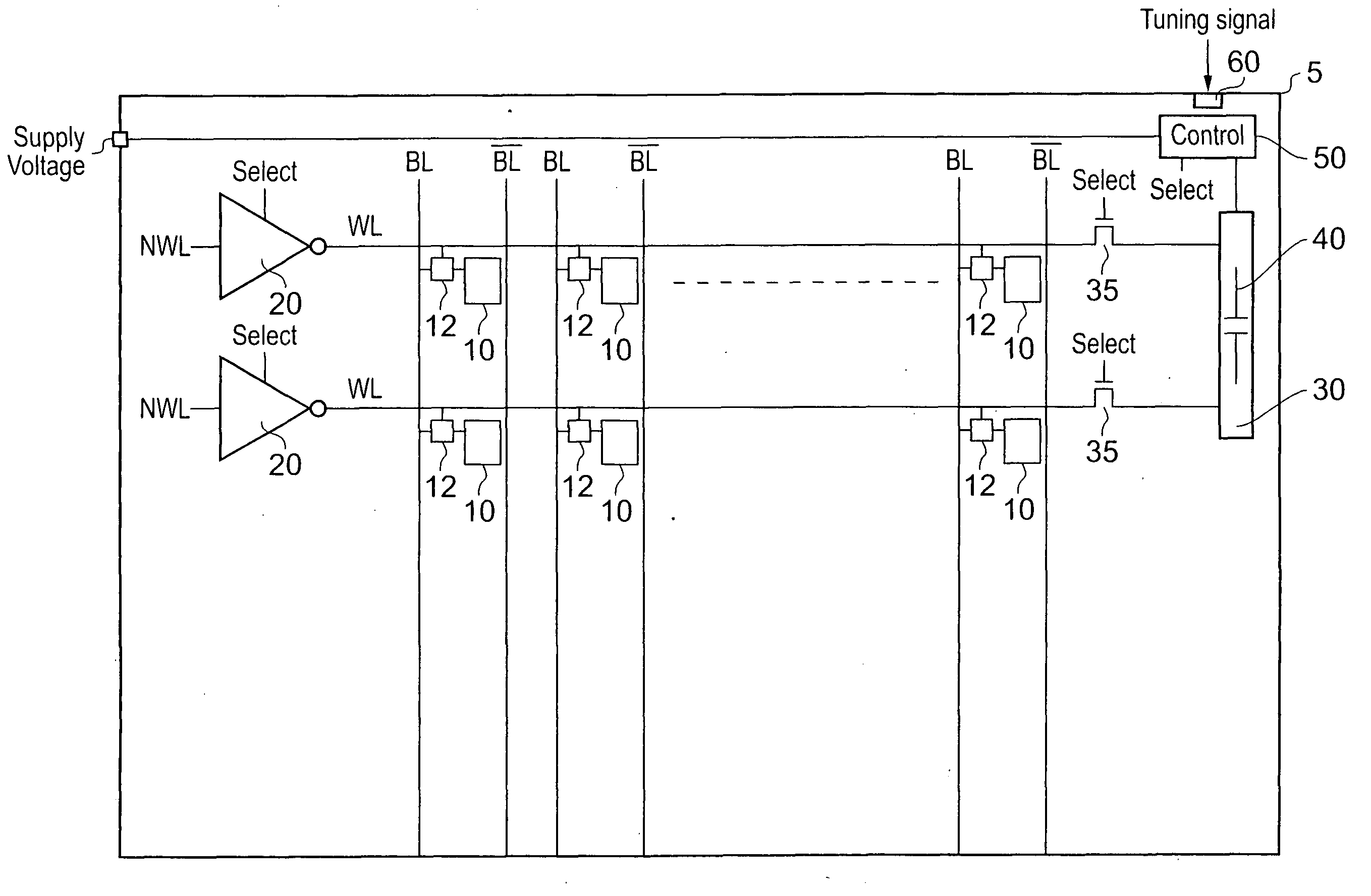
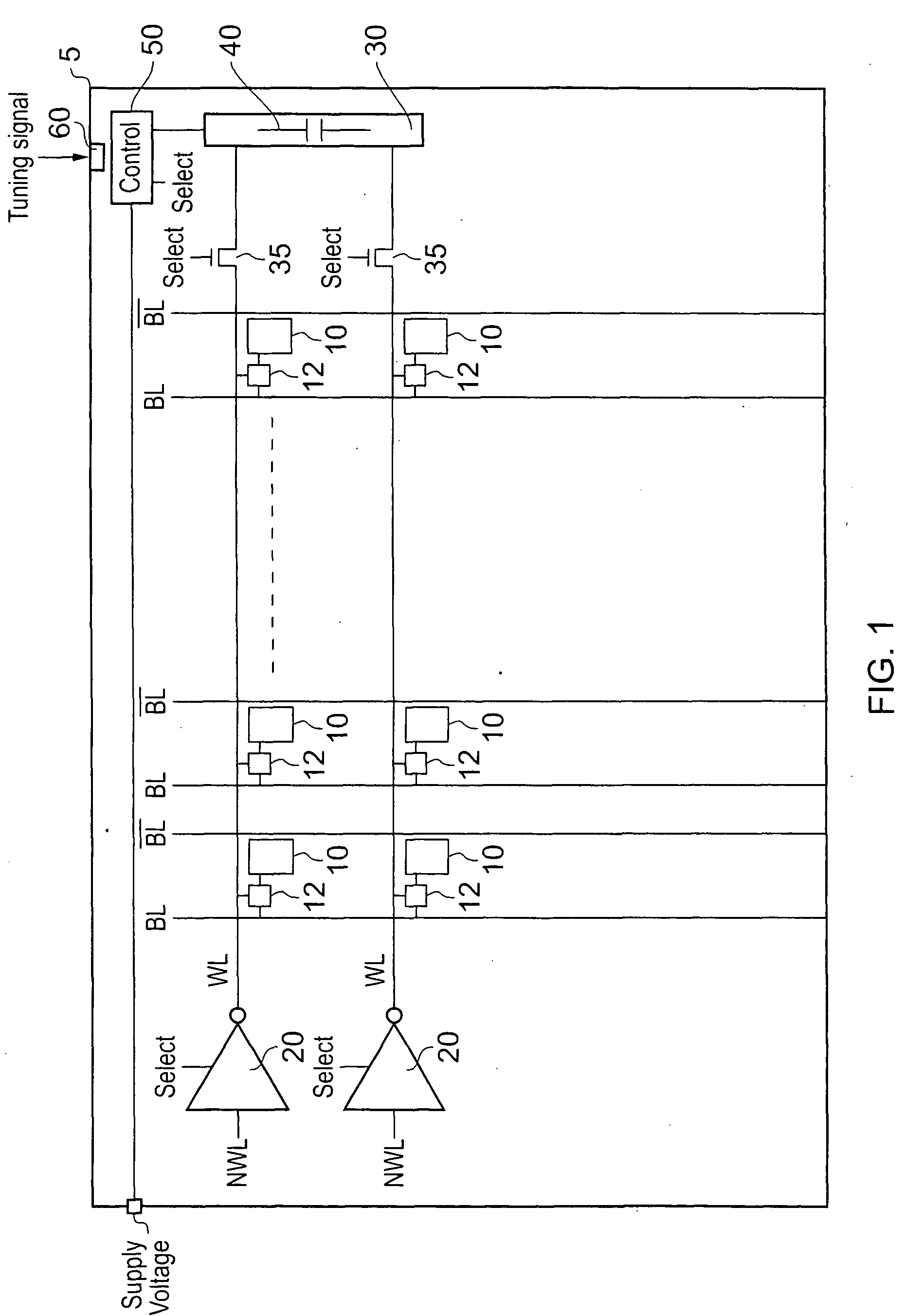
[0053]FIG. 1 shows a memory 5 according to an embodiment of the present invention. Memory 5 comprises a plurality of data storage cells 10 arranged in an array, each cell having access devices 12 controlling access to these storage cells. In this embodiment the memory is arranged as an array and requests to access data, access a selected row of the array via word lines WL.

[0054]In order to access a data storage cell 10 specified by a data access request a driver 20 on the relevant word line will be selected and it will power the word line to raise the voltage such that the access device 12 for cell 10 is turned on and access to the cell 10 via this device is provided. In this embodiment the memory is a SRAM memory with word lines and bit lines and complementary bit lines.

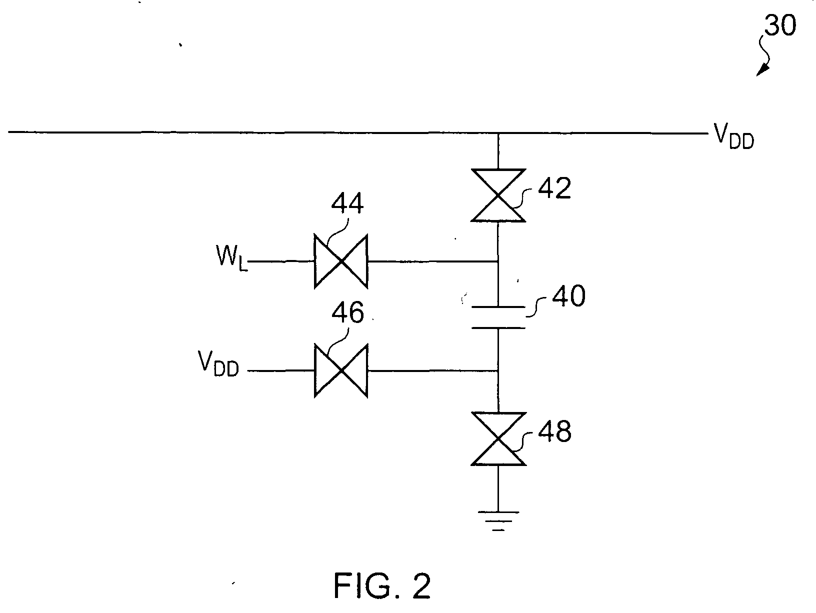
[0055]Memory 5 also comprises access control circuitry 30 which acts to change the voltage level supplied to the word line in response to a data access request in order to facilitate access to the storage cells.

[005...


PUM


Abstract

A semiconductor memory storage device is disclosed. This memory device has a plurality of storage cells for storing data; a plurality of access devices for allowing access to the corresponding plurality of storage cells, the plurality of access devices being arranged in at least two groups, each of the at least two groups being controlled by an access control line; access control circuitry for controlling a voltage level supplied to a selected one of at least two of the access control lines during access to the storage cell, the access control circuitry comprising a capacitor and switching circuitry; and control circuitry responsive to a data access request to access a selected storage cell to: connect a selected one of the access control lines to a voltage level to allow access via one of the access devices to the selected storage cell; and to control the switching circuitry of the access control circuitry to connect the capacitor of the access control circuitry to the selected access control line and thereby change the voltage level supplied to the selected access control line.

Description

BACKGROUND OF THE INVENTION[0001]1. Field of the Invention[0002]The field of the invention relates to the field of data storage and in particular, to the storage and access of data in semiconductor memories.[0003]2. Description of the Prior Art[0004]With ever increasing demands to reduce both the size of devices and their power consumption, it is becoming increasingly challenging to design robust semiconductor memories such as SRAM. Each storage cell in an SRAM comprises a feedback loop for holding a data value. In order to write to the feedback loop and store a new value, the input must have a high enough voltage level to be able to switch the state stored by the feedback loop if required, while reading from the feedback loop should be performed without disturbing the values stored in any of the feedback loops.[0005]As dimensions scale down the variations in device properties due to random dopant fluctuations, line edge roughness etc. increase drastically.[0006]Thus, designing a ro...

Claims


Application Information

Patent Timeline
Patent Type & Authority Applications(United States)
IPC IPC(8): G11C7/00G11C8/00
CPCG11C11/413
Inventor IDGUNJI, SACHIN SATISHGAJJEWAR, HEMANGI UMAKANTYEUNG, GUS
Owner ARM LTD
Why Eureka
Try Eureka