Vapor deposition system

Active Publication Date: 2011-06-02
TOKYO ELECTRON LTD
View PDF164 Cites 22 Cited by
  • Summary
  • Abstract
  • Description
  • Claims
  • Application Information

AI Technical Summary

Problems solved by technology

In addition, plasma excitation may activate film-forming chemical reactions that are not energetically or kinetically favored in thermal CVD.

Method used


Image

  • Vapor deposition system
  • Vapor deposition system
  • Vapor deposition system

Examples


Embodiment Construction

[0033]In the following description, in order to facilitate a thorough understanding and for purposes of explanation and not limitation, specific details are set forth, such as a particular geometry of the deposition system and descriptions of various components. However, it should be understood that the invention may be practiced in other embodiments that depart from these specific details.

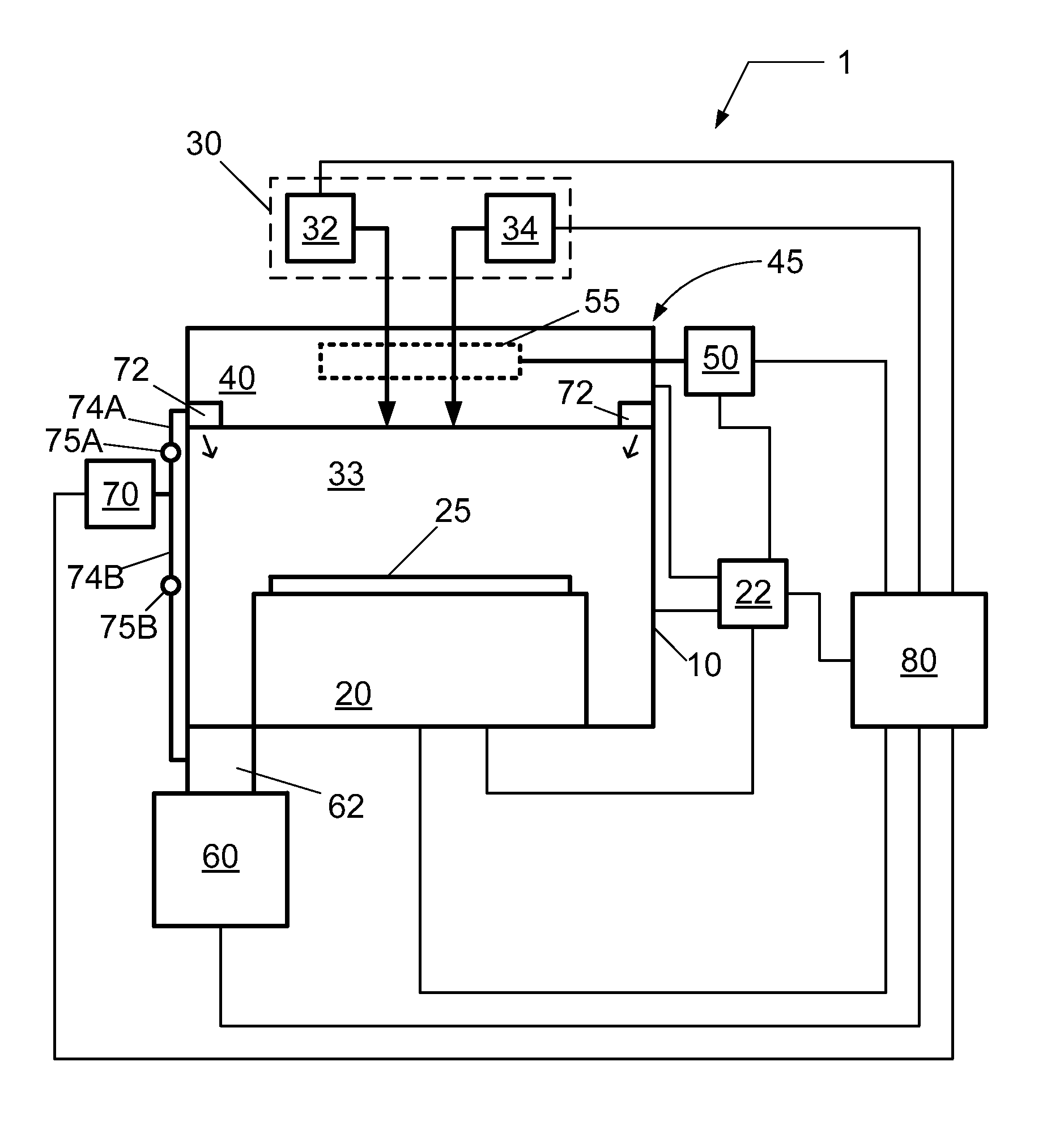
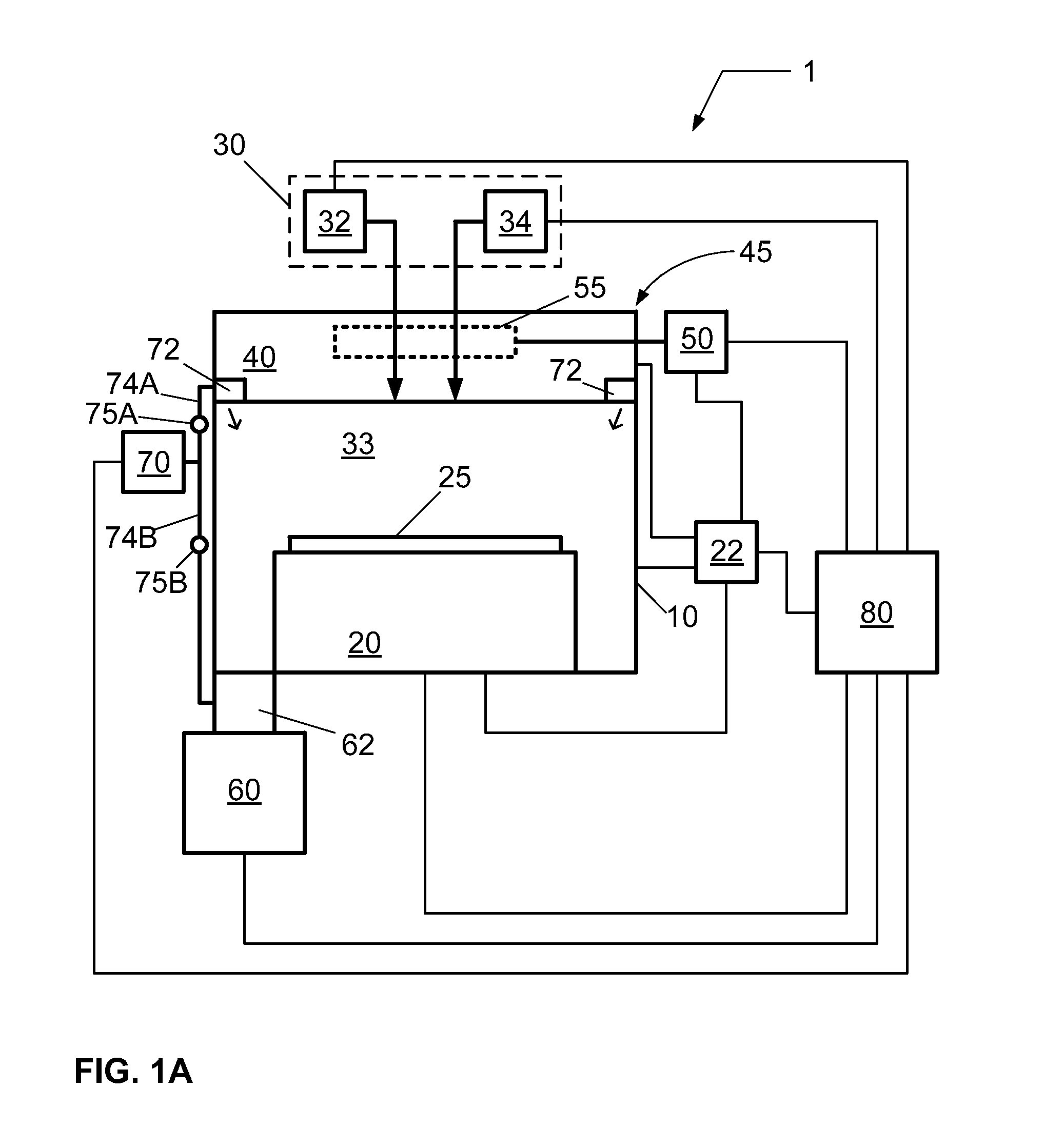
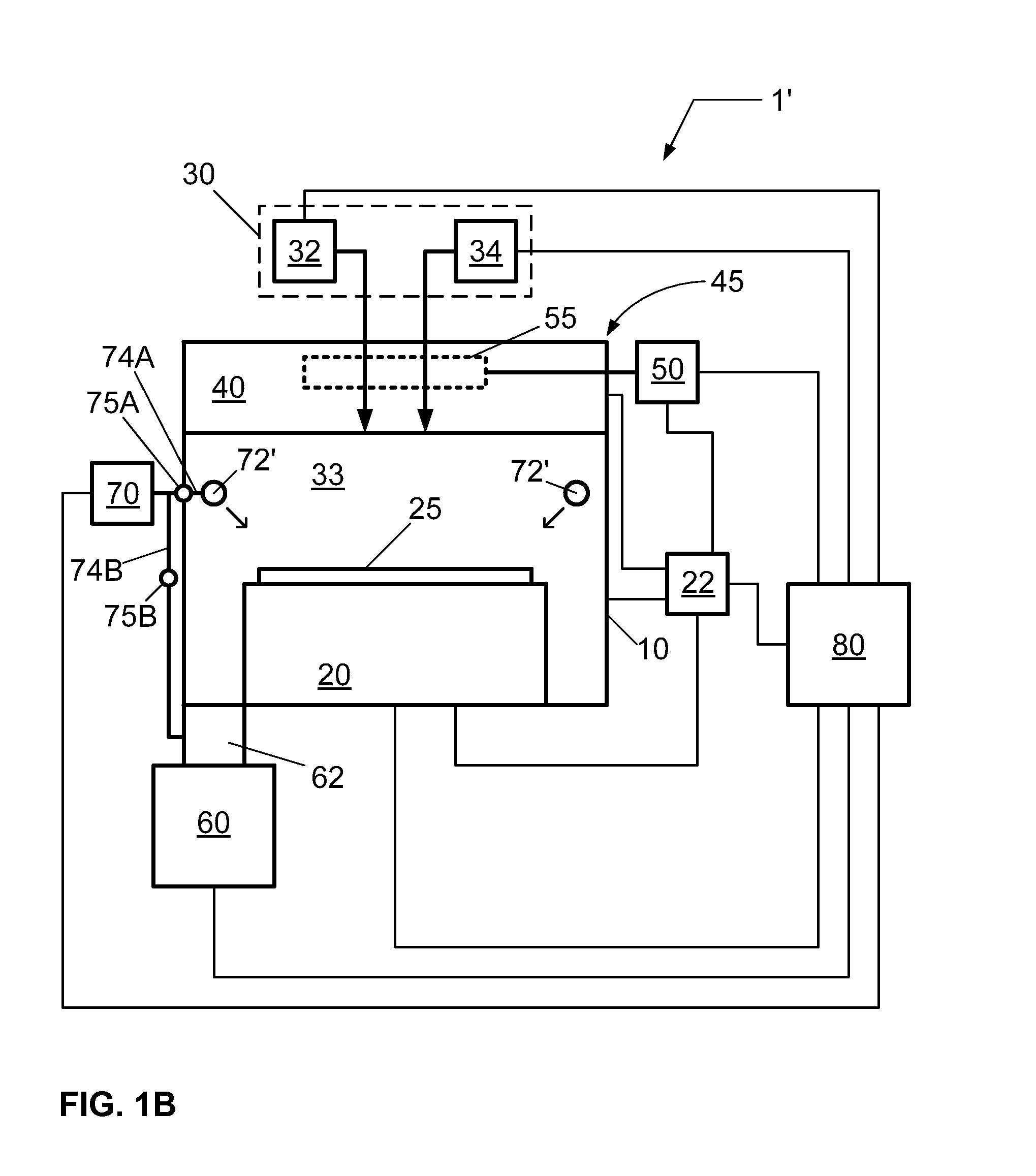
[0034]Referring now to the drawings, wherein like reference numerals designate identical or corresponding parts throughout the several views, FIGS. 1A and 1B schematically illustrate a deposition system (1, 1′) for depositing a thin film, such as a conductive film, a non-conductive film, or a semi-conductive film. For example, the thin film can include a dielectric film, such as a low dielectric constant (low-k) or ultra-low-k dielectric film. Deposition system (1, 1′) can include a chemical vapor deposition (CVD) system, whereby a film forming composition is thermally activated or decomposed in o...


PUM

PropertyMeasurementUnit
pressureaaaaaaaaaa
sizeaaaaaaaaaa
sizeaaaaaaaaaa

Abstract

A system for depositing a thin film on a substrate using a vapor deposition process is described. The deposition system includes a process chamber having a vacuum pumping system configured to evacuate the process chamber, a substrate holder coupled to the process chamber and configured to support the substrate, a gas distribution system coupled to the process chamber and configured to introduce a film forming composition to a process space in the vicinity of a surface of the substrate, a non-ionizing heat source separate from the substrate holder that is configured to receive a flow of the film forming composition and to cause thermal fragmentation of one or more constituents of the film forming composition when heated, and one or more power sources coupled to the heating element array and configured to provide an electrical signal to the at least one heating element zone. The deposition system further includes a remote source coupled to the process chamber and configured to supply a reactive composition to the process chamber to chemically interact with the substrate, wherein the remote source comprises a remote plasma generator, a remote radical generator, a remote ozone generator, or a water vapor generator, or a combination of two or more thereof.

Description

CROSS-REFERENCE TO RELATED APPLICATIONS[0001]This application is a continuation-in-part of U.S. Ser. No. 11 / 693,067, entitled “VAPOR DEPOSITION SYSTEM AND METHOD OF OPERATING”, and filed Mar. 29, 2007. The entire content of this application is herein incorporated by reference.BACKGROUND OF THE INVENTION[0002]1. Field of Invention[0003]The present invention relates to a system for thin film deposition, and more particularly to a system for depositing a thin film using a vapor deposition process.[0004]2. Description of Related Art[0005]During material processing, such as semiconductor device manufacturing for production of integrated circuits (ICs), vapor deposition is a common technique to form thin films, as well as to form conformal thin films over and within complex topography, on a substrate. Vapor deposition processes can include chemical vapor deposition (CVD) and plasma enhanced CVD (PECVD). For example, in semiconductor manufacturing, such vapor deposition processes may be us...

Claims


Application Information

Patent Timeline
Patent Type & Authority Applications(United States)
IPC IPC(8): C23C16/503C23C16/50
CPCC23C16/4557C23C16/452B05D1/60C23C16/44C23C16/45561C23C16/45563C23C16/45565C23C16/487C23C16/50
Inventor FAGUET, JACQUESLEE, ERIC M.
Owner TOKYO ELECTRON LTD
Why Eureka
Try Eureka