
Circuit pattern examining apparatus and circuit pattern examining method

a circuit pattern and circuit pattern technology, applied in the direction of semiconductor/solid-state device testing/measurement, image enhancement, instruments, etc., can solve the problems of high defect density, difficult photolithography process production, device defect, etc., and achieve high sensitivity

Active Publication Date: 2011-06-02
HITACHI HIGH-TECH CORP
View PDF15 Cites 13 Cited by
  • Summary
  • Abstract
  • Description
  • Claims
  • Application Information

AI Technical Summary

Benefits of technology

[0009]According to the present invention, an inspection technique which can judge defects with high sensitivity in the outer-most periphery of the memory mat of semiconductor device and even in the peripheral circuit without repetiveness as well is realized.

Problems solved by technology

On the other hand, in a peripheral circuit other than the memory mat, even a single defect causes the device defective and so the pattern dimension is not so miniaturized as in the case of the memory mat.
Especially, at the outer-most of the memory mat, the pattern density changes abruptly and hence, production in photolithography process is very difficult and the defect density is very high.
But a technique capable of detecting defects in both of them at a same time with high accuracies has not yet been known.

Method used


Image

  • Circuit pattern examining apparatus and circuit pattern examining method
  • Circuit pattern examining apparatus and circuit pattern examining method
  • Circuit pattern examining apparatus and circuit pattern examining method

Examples


Embodiment Construction

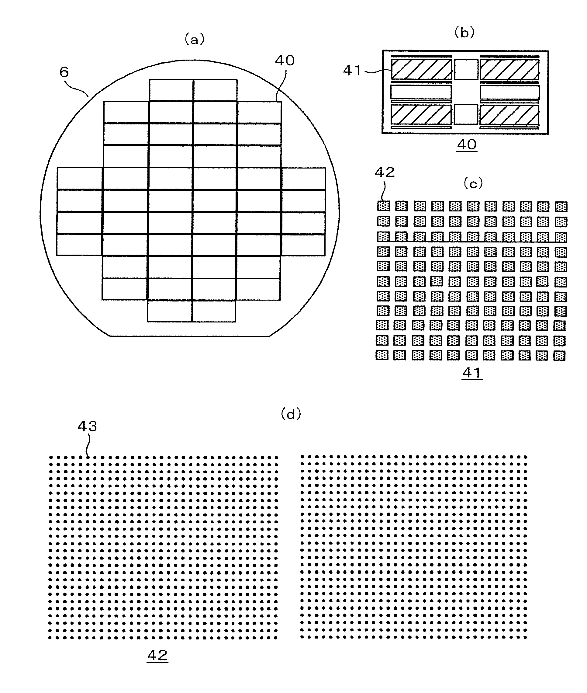
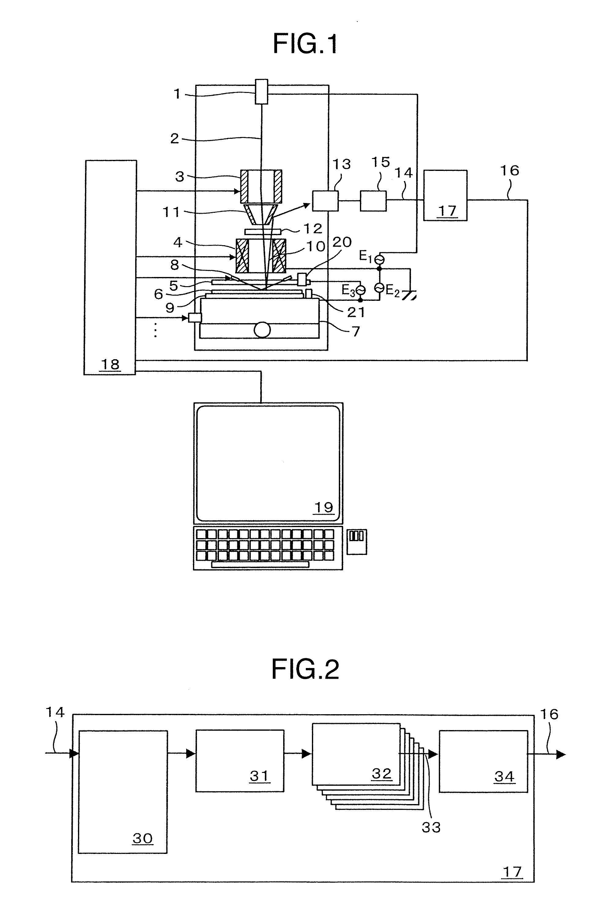
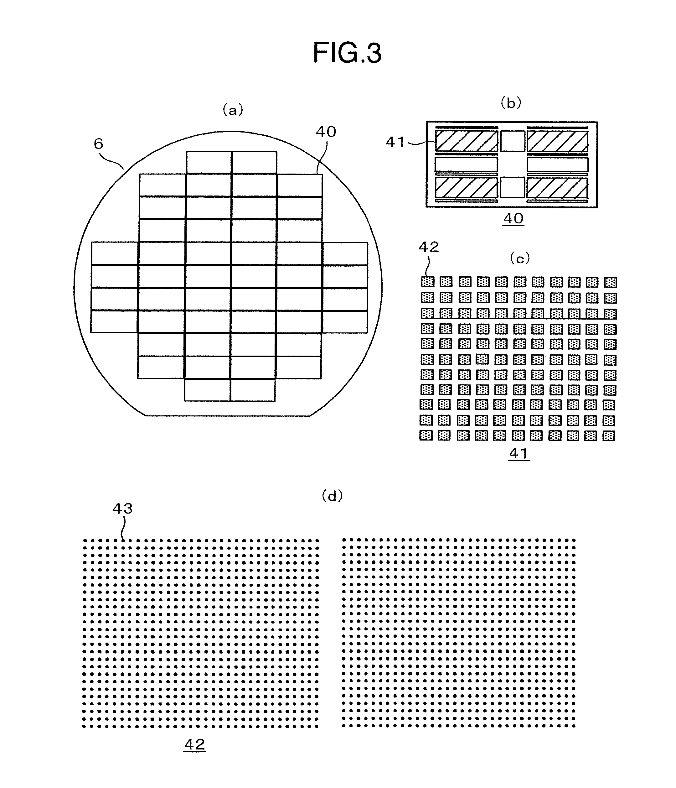
[0023]An embodiment of the present invention will now be described with reference to the drawings. FIG. 1 is a diagram showing the overall configuration of a circuit pattern inspection apparatus, illustrating a principal portion in a cross-sectional form. In the present embodiment, an inspection apparatus will be described. It is a scanning electron microscope adapted to obtain an image by irradiating an electron beam on a sample. The principal portion of the invention is same when light is used in place of the election beam. Therefore, a description will not be given herein of an embodiment of an optical inspection apparatus.

[0024]In FIG. 1, electrons 2 come from an electron source 1 irradiate a semiconductor wafer 6. The electrons 2 are focused finely by an objective lens 4 and are deflected by a deflector 3 so as to scan the surface of semiconductor wafer 6. Since the semiconductor wafer 6 that is under irradiation of the electrons 2, are charged up and an image to be obtained wi...


PUM


Abstract

Provided is an examination technique to detect defects with high sensitivity at an outer-most repeative portion of a memory mat of a semiconductor device and even in a peripheral circuit having no repetitiveness.A circuit pattern inspection apparatus comprises an image detection unit for acquiring an image of a circuit pattern composed of multiple die having a repeative pattern, a defect judgement unit which composes, in respect of an acquired detected image, reference images by switching addition objectives depending on regions of repeative pattern and the other regions and compares a composed reference image with the detected image to detect a defect, and a display unit for displaying the image of the detected defect.

Description

TECHNICAL FIELD[0001]The present invention relates to a technique to inspect a substrate unit having a circuit pattern of, for example, a semiconductor device or liquid crystals by utilizing light or an electron beam.BACKGROUND ART[0002]An inspection apparatus for a circuit pattern of a semiconductor device or liquid crystals has the function to compare an image obtained under irradiation of light or an electron beam with a reference image represented by a standard image or an adjoining image, extract a pixel affected by a difference to judge it as a defect and output a coordinate thereof.[0003]In a circuit pattern as a target of the inspection apparatus, the pattern density per unit area has been quadrupping every 3 years. This is realized by the pattern shrinkage. The shrinkage causes the difference between a defect and a normal portion becomes very small. Then, by setting a threshold value between a signal value of the defect and that of the normal portion and discriminating the ...

Claims


Application Information

Patent Timeline
Patent Type & Authority Applications(United States)
IPC IPC(8): G06K9/00
CPCG01N21/9501G01N21/95607H01L22/12G06T2207/10061G06T2207/30148G06T7/001
Inventor HIROI, TAKASHIYOSHIDA, TAKEYUKIHOSOYA, NAOKIHONDA, TOSHIFUMI
Owner HITACHI HIGH-TECH CORP
Learn More