Method for Manufacturing Micro-Channel, Die for Molding Micro-Channel Chip, and Micro-Channel Chip

Inactive Publication Date: 2011-06-09
KONICA MINOLTA OPTO
View PDF6 Cites 1 Cited by
  • Summary
  • Abstract
  • Description
  • Claims
  • Application Information

AI Technical Summary

Benefits of technology

[0021]A micro-channel chip molding die according to the present invention has a constitution in which a convex or concave section longer than a micro-channel constituted in a cavity is provided. A micro-channel chip manufacturing method according to the present invention has a constitution in which a micro-channel is removed from a die and thereafter a concave or convex section is removed. Thereby, no micro-channel is removed lastly, whereby the reduction of a force due to molding shrinkage applied to the micro-channel is realized. Therefore, releasing deformation in the edge of the micro-channel is reduced and then an accurate micro-channel can be molded and also excellent flatness can be achieved.
[0022]Further, a convex or concave section longer than a micro-channel is provided in a portion other than the portion where joining to another resin substrate is made, whereby the effect of releasing deformation in the concave or convex section against the joining portion can be reduced.
[0023]Still further, a micro-channel chip according to the present invention is manufactured via accurate joining in which a resin substrate featuring high flatness is used, and the chip has an accurate micro-channel. Thereby, the micro-channel chip according to the present invention exhibits improved quantitative performance and reproducibility.

Problems solved by technology

However, such glass substrates are unsuitable for mass production and exhibit extremely high cost.

Method used


Image

  • Method for Manufacturing Micro-Channel, Die for Molding Micro-Channel Chip, and Micro-Channel Chip
  • Method for Manufacturing Micro-Channel, Die for Molding Micro-Channel Chip, and Micro-Channel Chip
  • Method for Manufacturing Micro-Channel, Die for Molding Micro-Channel Chip, and Micro-Channel Chip

Examples


modified example 1

[0057]Next, Modified Example 1 of the above micro-channel chip manufacturing method and the micro-channel chip molding die used therefor will now be described with reference to FIG. 6 and FIG. 7. FIG. 6 is a schematic cross-sectional view in which a resin has been injected into a micro-channel chip molding die according to Modified Example 1. And, FIG. 7 is a schematic cross-sectional view of the moment when the micro-channel chip molding die according to Modified Example 1 is released from a molded resin substrate. In this modified example, as a structure to reduce releasing deformation of a micro-channel 002, a micro-channel chip molding die provided with a anti-shrinkage concave section will be described.

[0058]As shown in FIG. 6, a micro-channel chip molding die 100 according to Modified Example 1 has a anti-shrinkage concave section 200 toward the direction opposed to the cavity. The length (depth) of this anti-shrinkage concave section 200 in the direction opposed to the cavity...

modified example 2

[0064]Further, Modified Example 2 of the above micro-channel chip manufacturing method and the micro-channel chip molding die used therefor will now be described with reference to FIG. 8 and FIG. 9. FIG. 8 is a schematic cross-sectional view in which a resin has been injected into a micro-channel chip molding die according to Modified Example 2. FIG. 9 is a schematic cross-sectional view in which the micro-channel chip molding die according to Modified Example 2 has been released from a molded resin substrate. In this modified example, a micro-channel chip molding die provided with a structure in which releasing deformation in a anti-shrinkage concave section is absorbed will be described.

[0065]As shown in FIG. 8, the micro-channel chip molding die 100 according to the present modified example has a constitution in which a anti-deformation convex section 300 is provided in the boundary portion of the anti-shrinkage convex section 103 and the molding transfer surface 101. In the pres...

example 1

[0070]Next, specific Example 1 will now be described.

[0071]In Example 1, based on the method according to the embodiment, a micro-channel chip was produced. Initially, to produce a resin substrate 001, a micro-channel chip molding die 100 was produced specifically as follows:

[0072]Resin material: PMMA

[0073]Melting temperature t1=250° C.

[0074]Melting temperature t2=93° C.

[0075]The height of the highest portion of the cavity direction in the micro-structure 102 (the depth of the deepest portion of the micro-channel 002) d1=50 μm

[0076]The height of the anti-shrinkage convex section 103 d2=60 μm

[0077]The size of the anti-shrinkage convex section=0.003 mm2

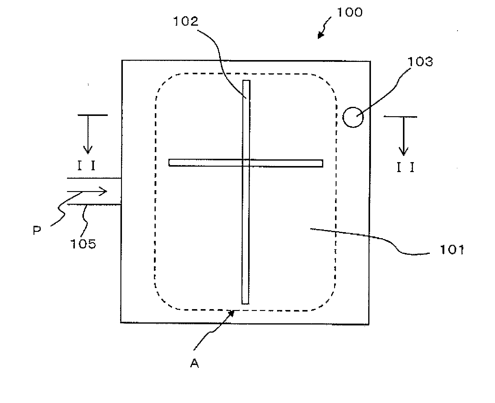
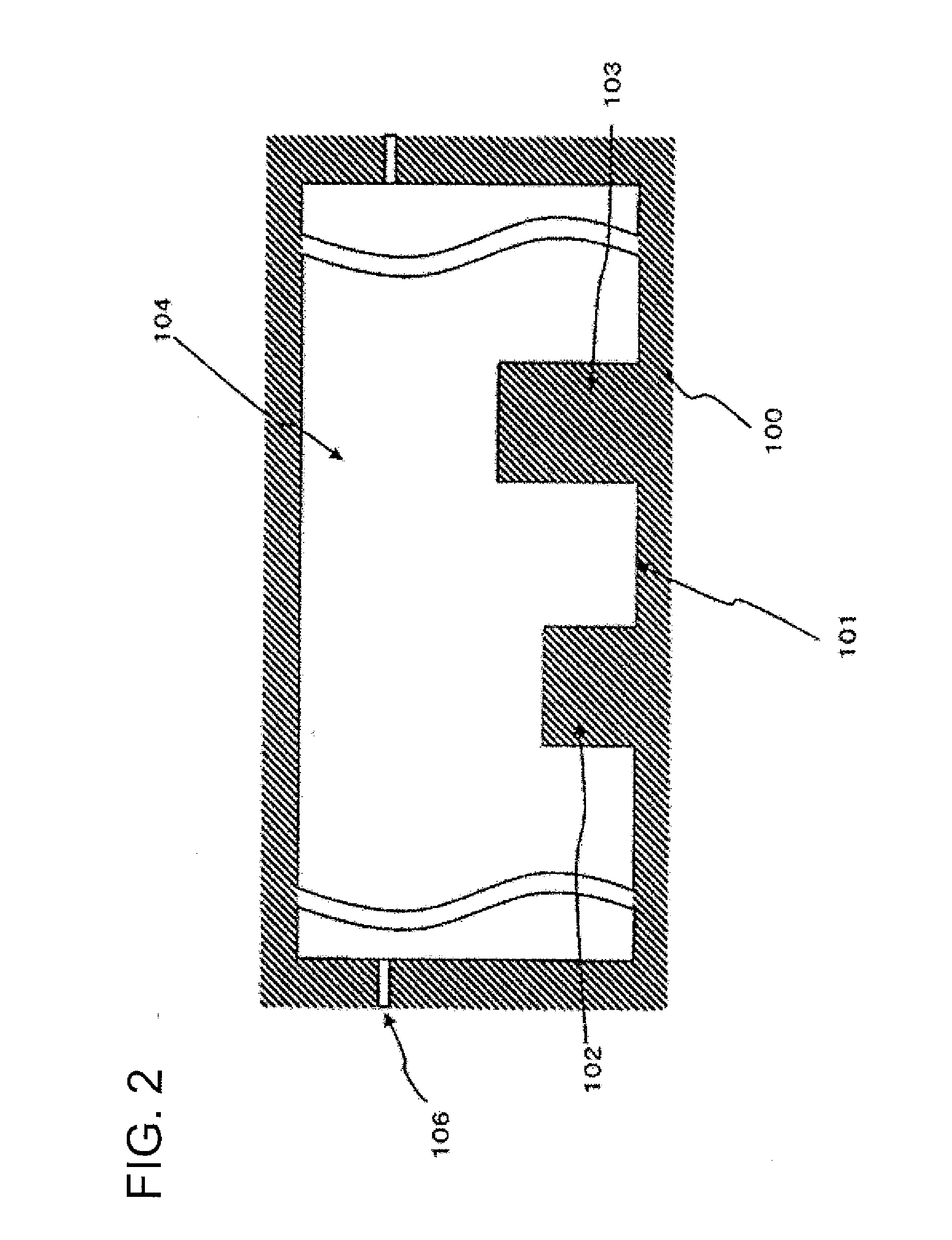
[0078]The location of the anti-shrinkage convex section 103=the symbol 103 in FIG. 3

[0079]Then, using an injection molding machine employing the micro-channel chip molding die 100, PMMA, a transparent resin material, was molded to produce a resin substrate 001 in which on the surface of a 30 mm square plate-shaped member having a thick...


PUM

PropertyMeasurementUnit
Lengthaaaaaaaaaa
Structureaaaaaaaaaa
Heightaaaaaaaaaa

Abstract

A die (100) is provided with: a cavity which can contain a molten resin; a micro-structure (102) provided on a molding transfer surface (101) forming the cavity such that the fine structure protrudes to the cavity side from the molding transfer surface (101); and a anti-shrinkage convex section (103) protruding higher than the micro-structure (102) to the cavity side from one surface. A molten resin is applied to the die (100) and the surface of the die is relatively removed in the order of the micro-structure (102) and the anti-shrinkage convex section (103) from a resin substrate (001) formed by solidifying the resin.

Description

TECHNICAL FIELD[0001]The present invention relates to a micro-channel chip manufacturing method by joining a resin substrate in which a micro-channel is formed, a micro-channel chip molding die used for the manufacturing, and a micro-channel chip manufactured by the manufacturing method.BACKGROUND[0002]Devices referred to as microanalysis chips or μTAS (Micro Total Analysis Systems) have been put to practical use, in which using a microfabrication technology, micro-channels and circuits are formed on a silicon or glass substrate, and thereby chemical reaction, separation, or analysis is carried out in a micro-space by introducing a liquid sample such as a nucleic acid, protein, or blood into such micro-channels. It is conceivable that these micro-channel chips have such advantages that the used amount of a sample or a reagent or the discharge amount of waste liquid is reduced, and small-foot print, portable, and inexpensive systems are realized.[0003]Micro-channel chips are manufact...

Claims


Application Information

Patent Timeline
IPC IPC(8): B29C45/16
CPCB01L3/502707B01L2200/10B01L2200/12B01L2300/044B29C45/0025B29C45/263B81B2201/051B81B2203/0338B81C1/0046B01L2300/12B29C33/42B29C45/37B29C45/40
Inventor SEKIHARA, KANJI
Owner KONICA MINOLTA OPTO
Why Eureka
Try Eureka