Semiconductor Light Emitting Device

a technology of semiconductors and light-emitting devices, which is applied in the direction of semiconductor devices, electrical devices, nanotechnology, etc., can solve the problems of difficult to obtain as good device characteristics as expected, complicate the manufacturing process, and cannot be fundamentally solved

Active Publication Date: 2011-06-16
WOOREE E&L
View PDF7 Cites 16 Cited by
  • Summary
  • Abstract
  • Description
  • Claims
  • Application Information

AI Technical Summary

Problems solved by technology

The first method generates a lot of defects during the manufacture of the device due to less-advanced growth techniques for a hetero crystal growth direction, which makes it difficult to obtain as good device characteristics as expected.
Additionally, it complicates the manufacturing process [K. Nishizuka et

Method used


Image

  • Semiconductor Light Emitting Device
  • Semiconductor Light Emitting Device
  • Semiconductor Light Emitting Device

Examples


Embodiment Construction

[0019]The present disclosure will now be described in detail with reference to the accompanying drawings.

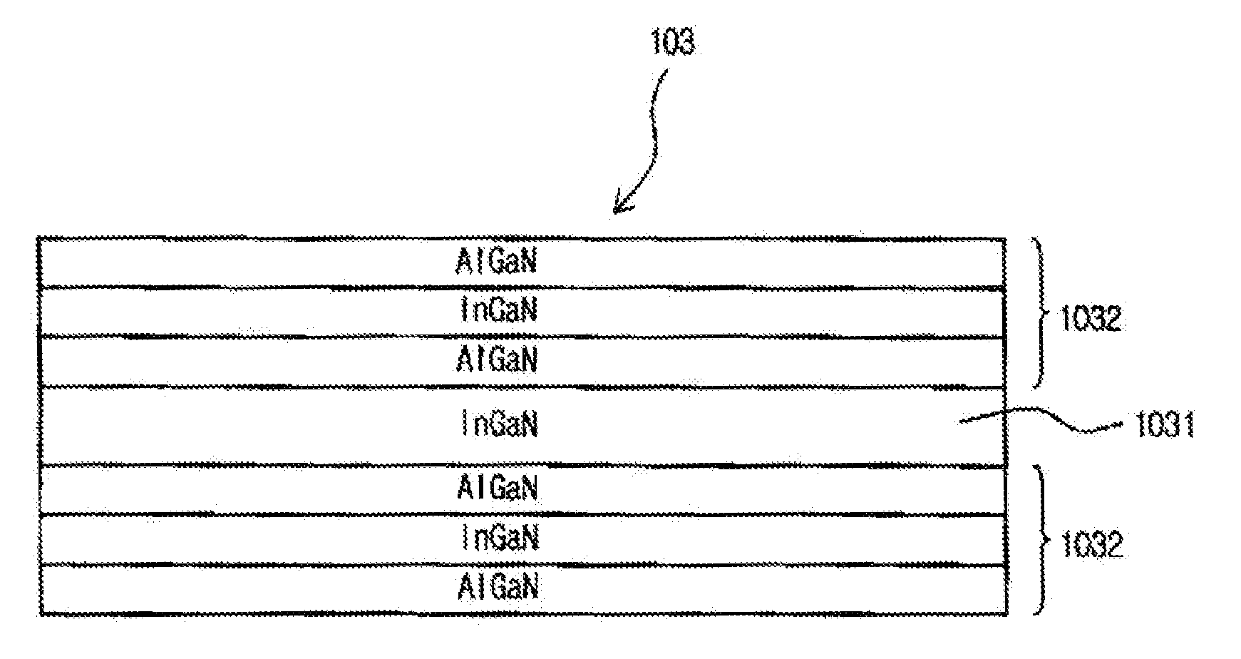
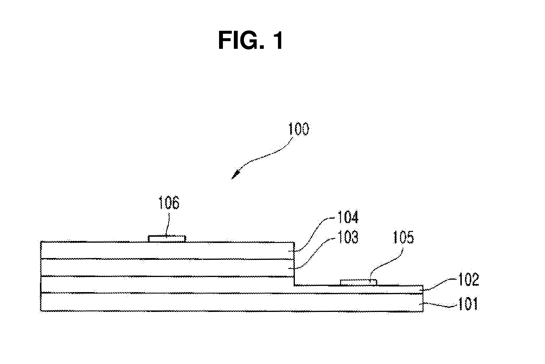
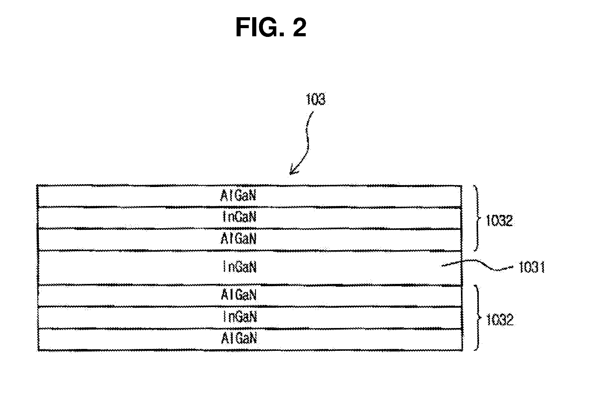
[0020]FIG. 1 is a schematic sectional view of a semiconductor light-emitting device according to an exemplary embodiment of the present invention, and FIG. 2 is a sectional view of a light-emitting layer shown in FIG. 1.

[0021]Referring to FIGS. 1 and 2, the semiconductor light-emitting device 100 according to the exemplary embodiment of the present invention includes an N-type contact layer 102, a light-emitting layer 103, and a P-type contact layer 104.

[0022]The N-type contact layer 102 may be formed on a substrate 101. For example, the substrate 101 may be an Al2O3 substrate or an SIC substrate. Optionally, a buffer layer (not shown) may be further formed between the substrate 101 and the N-type contact layer 102. The buffer layer is provided for facilitating the high-quality nitride crystal growth.

[0023]For example, the N-type contact layer 102 may be provided as one or more n...


PUM


Abstract

The present disclosure relates to a semiconductor light-emitting device which includes: a light-emitting layer composed of an active layer and of barrier layers formed as superlattice layers and disposed on and under the active layer to relieve stresses applied to the active layer and reduce the sum of electric fields generated in the active layer by the spontaneous polarization and the piezo; an N-type contact layer injecting electrons into the light-emitting layer; and a P-type contact layer disposed opposite to the N-type contact layer with respect to the light-emitting layer and injecting holes into the light-emitting layer, wherein the active layer contains InGaN, and the barrier layers are formed by alternately stacking of an AlGaN thin film and an InGaN thin film.

Description

TECHNICAL FIELD[0001]The present invention relates to a semiconductor light-emitting device, and more particularly, to a semiconductor light-emitting device which reduces an internal electric field to improve light-emitting efficiency[0002]Here, the semiconductor light-emitting device indicates a semiconductor light-emitting device which generates light by recombination of electrons and holes, and its example is a III-nitride semiconductor light-emitting device. The III-nitride semiconductor is made of a compound containing Al(x)Ga(y)In(1-x-y)N (0≦x≦1, 0≦y≦1, 0≦x+y≦1). Another example is a GaAs semiconductor light-emitting device used for red emission.BACKGROUND ART[0003]This section provides background information related to the present disclosure which is not necessarily prior art.[0004]It has been known that III-V nitride and II-VI compound semiconductor structures, which constitute blue-violet and blue-green semiconductor light-emitting devices, significantly deteriorate a light...

Claims


Application Information

Patent Timeline
IPC IPC(8): H01L33/06
CPCB82Y20/00H01L33/32H01L33/14H01L33/06
Inventor JANG, JUNG TAEKOO, BUN HEIAHN, DO YEOLPARK, SEOUNG HWAN
Owner WOOREE E&L
Why Eureka
Try Eureka