Method of manufacturing piezoelectric device

Active Publication Date: 2011-06-23
MURATA MFG CO LTD
View PDF5 Cites 21 Cited by
  • Summary
  • Abstract
  • Description
  • Claims
  • Application Information

AI Technical Summary

Benefits of technology

[0021]In this case, the temperature characteristic of the resona

Problems solved by technology

Depending upon the method used to form the through-hole, problems such as the time re

Method used


Image

  • Method of manufacturing piezoelectric device
  • Method of manufacturing piezoelectric device
  • Method of manufacturing piezoelectric device

Examples


Example

[0028]Hereinafter, preferred embodiments of the present invention will be described with reference to the drawings.

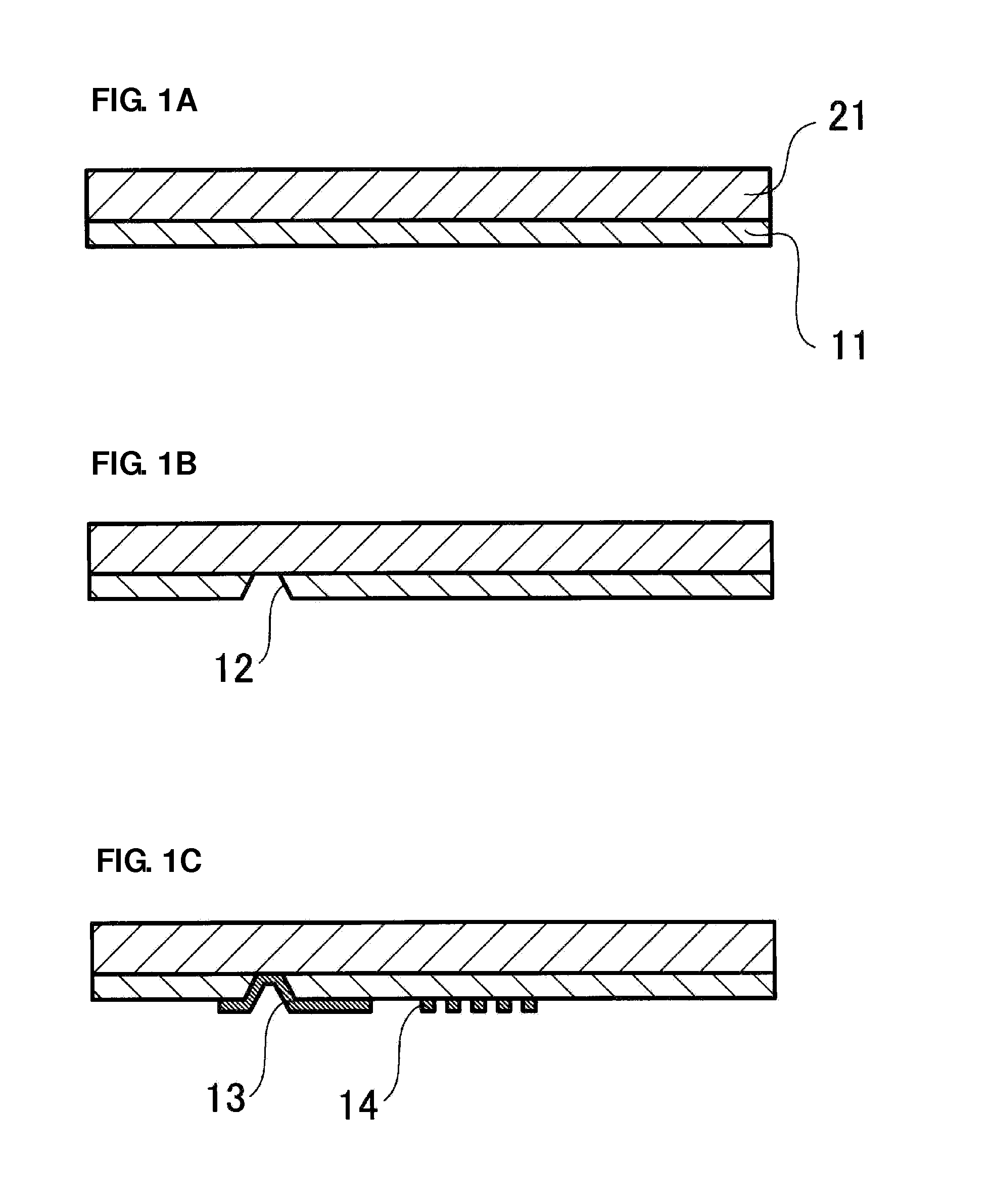
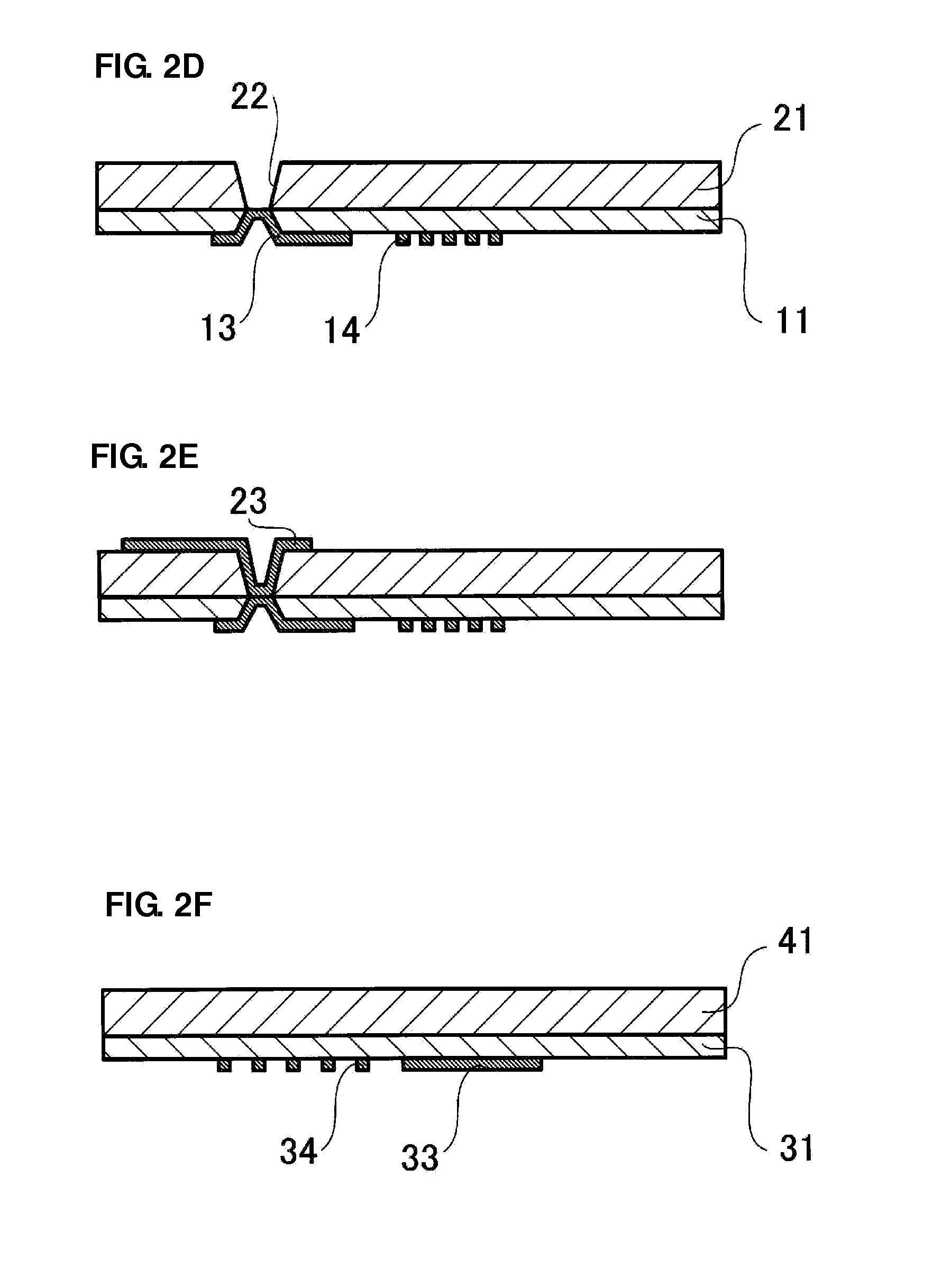
[0029]FIGS. 1A to 3G are sectional views illustrating a method of manufacturing a piezoelectric device according to a preferred embodiment of the present invention.

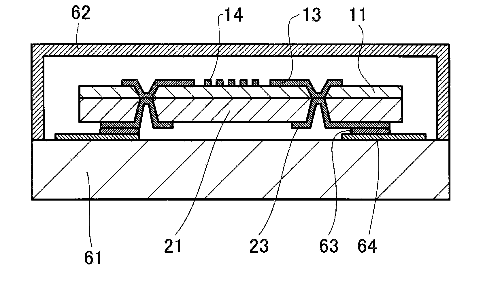
[0030]First, as shown in FIG. 1A, a first substrate 11 and a second substrate 21 having a toughness greater than that of the first substrate 11 are bonded together. The first substrate 11 may preferably be thinned by, for example, polishing after being bonded to the second substrate 21 to obtain a predetermined thickness. The first substrate 11 is preferably a piezoelectric substrate, for example. Examples of the material for the first substrate 11 preferably include lithium tantalate, lithium niobate, lithium borate, langasite, and crystal. In addition, since a single-crystal substrate has a relatively low toughness, using a single-crystal substrate as the first substrate 11 is especially effective and prefe...


PUM

PropertyMeasurementUnit
Expansion enthalpyaaaaaaaaaa

Abstract

A method of manufacturing a piezoelectric device includes the steps of bonding a first substrate to a second substrate having a toughness greater than that of the first substrate, forming a first though-hole through the first substrate from the side opposite to the side on which the second substrate is bonded, and forming a second through-hole through the second substrate at a location corresponding to the first through-hole by a formation method different from that used to form the first through-hole from the side opposite to the side on which the first substrate is bonded.

Description

BACKGROUND OF THE INVENTION[0001]1. Field of the Invention[0002]The present invention relates to a method of manufacturing a piezoelectric device, and more particularly, to a method of manufacturing a piezoelectric device including a piezoelectric substrate that is bonded to another substrate.[0003]2. Description of the Related Art[0004]A circuit section of a wireless communication device, such as a cellular phone, for example, requires an interstage filter and a duplexer. Piezoelectric devices have been used in interstage filters and duplexers in the past. Examples of the piezoelectric devices include elastic wave devices, such as a surface acoustic wave (SAW) device and a boundary acoustic wave device, bulk acoustic wave (BAW) devices, film bulk acoustic resonators (FBAR), and other suitable devices. These piezoelectric devices include a piezoelectric substrate.[0005]An example of a known piezoelectric device is described, for example, in Japanese Unexamined Patent Application Pub...

Claims


Application Information

Patent Timeline
IPC IPC(8): H01L41/22H01L41/09H01L41/18H01L41/312H01L41/332H03H3/08H03H9/145H03H9/25
CPCH03H3/02H03H9/02574H03H9/1014H03H9/1071Y10T29/49165Y10T29/49126Y10T29/42Y10T156/1056Y10T156/1057
Inventor MIYAKE, TAKASHITOYOTA, YUJI
Owner MURATA MFG CO LTD
Why Eureka
Try Eureka