

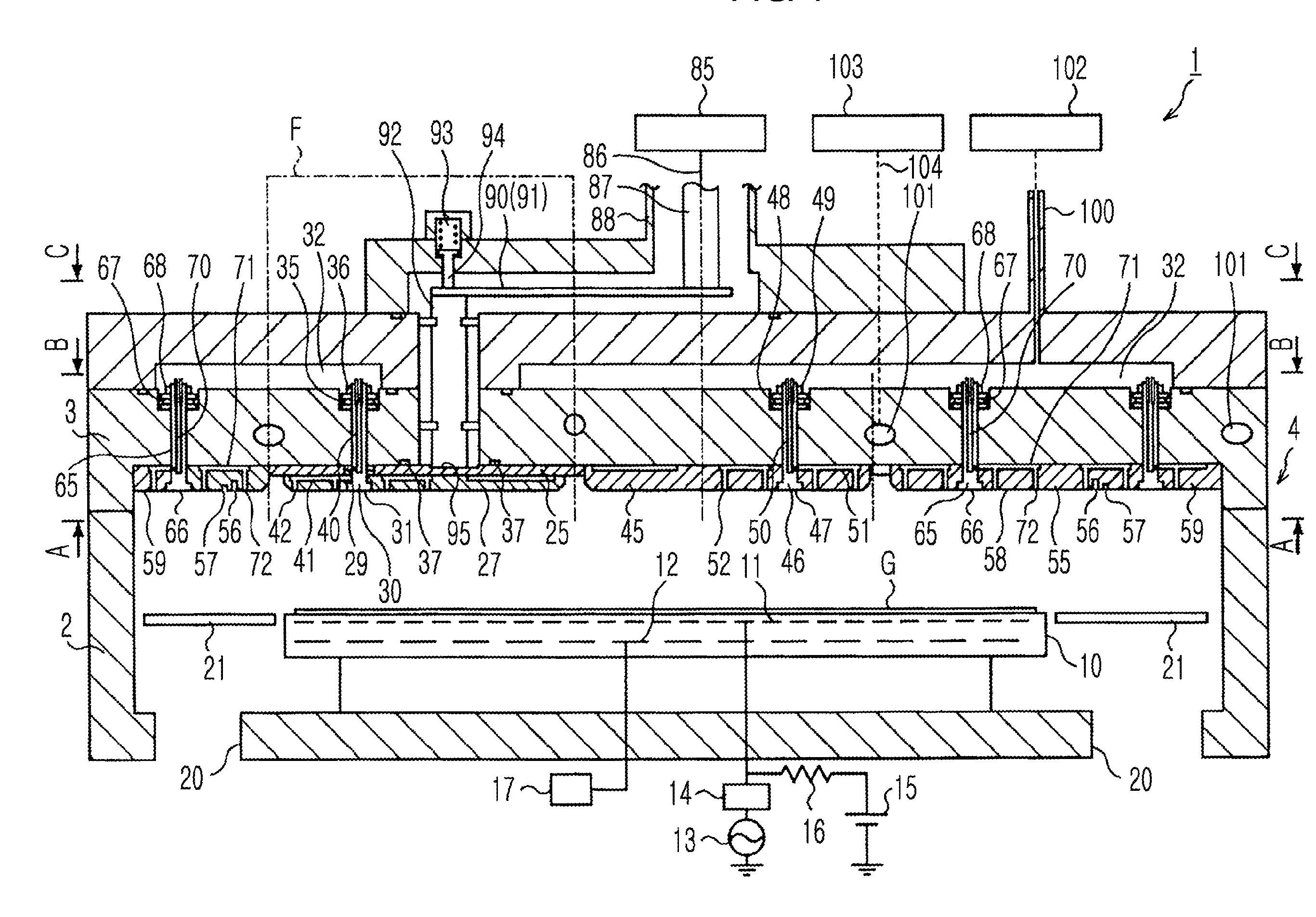
Plasma processing apparatus
a processing apparatus and plasma technology, applied in the field of plasma processing apparatus, can solve the problems of increasing the size of the substrate, increasing the cost, increasing the use amount of the dielectric, etc., and achieve the effects of reducing the amount of dielectric used, reducing the area of the exposed part, and generating metal contamination
- Summary
- Abstract
- Description
- Claims
- Application Information
AI Technical Summary
Benefits of technology
Problems solved by technology
Method used
Image

Examples
modified examples
[0184]Hereinafter, the plasma processing apparatus 1 according to other embodiments will be described. Also, like reference numerals denote like elements as those of the plasma processing apparatus 1 described above with reference to FIG. 1, or the like, so as to omit overlapping descriptions.
modified example 1
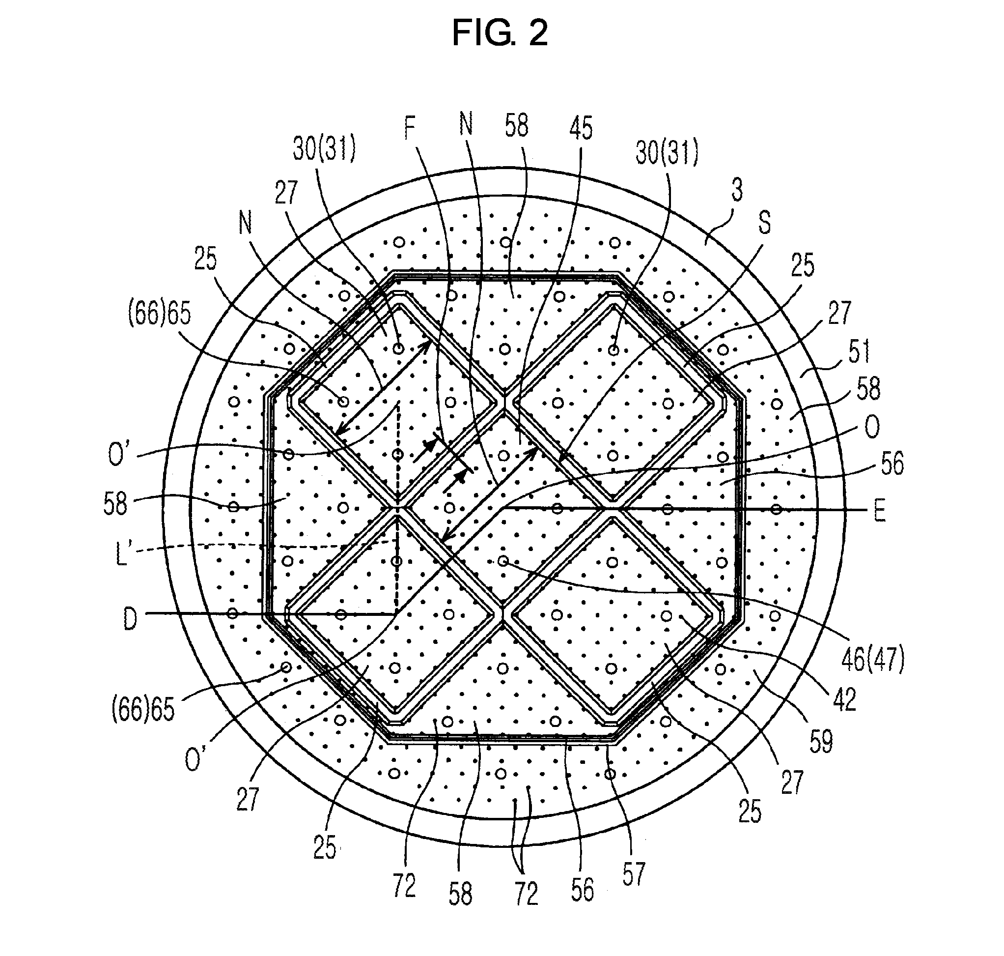
[0185]FIG. 15 is a view of a lower surface of the lid 3 of the plasma processing apparatus 1 according to Modified Example 1. In the plasma processing apparatus 1 according to Modified Example 1, 8 dielectrics 25 formed of, for example, Al2O3, are attached to the lower surface of the lid 3. Like above, as shown in FIG. 7, each dielectric 25 has a plate shape that may be considered substantially as a square. Each dielectric 25 is disposed in such a way that vertical angles are adjacent to each other. Also, the vertical angles of each dielectric 25 are disposed to be adjacent to each other on the line L′ connecting the center points O′ of the neighboring dielectrics 25. As such, by adjoining the vertical angles of each of the 8 dielectrics 25, and by disposing the vertical angles of each dielectric 25 adjacent to each other on the line connecting the center points O′ with respect to the neighboring dielectrics 25, the square region S surrounded by the 4 dielectrics 25 is formed on 3 p...
modified example 2
[0197]FIG. 16 is a longitudinal-sectional view (a cross-sectional view taken along a line D-O′-O-E of FIG. 17) showing a schematic configuration of the plasma processing apparatus 1 according to Modified Example 2. FIG. 17 is a cross-sectional view taken along a line A-A of FIG. 16. In the plasma processing apparatus 1 according to Modified Example 2, 8 dielectrics 25 formed of, for example, Al2O3, is attached to the lower surface of the lid 3. Like above, as shown in FIG. 7, each dielectric 25 has a plate shape that may be considered substantially as a square. The vertical angles of each dielectric 25 are disposed to be adjacent to each other. Also, the vertical angles of each dielectric 25 are disposed to be adjacent to each other on the line L′ connecting the center points O′ of the neighboring dielectrics 25. As such, by adjoining the vertical angles of each of the 8 dielectrics 25, and by disposing the vertical angles of each dielectric 25 to be adjacent to each other on the li...
PUM
| Property | Measurement | Unit |
|---|---|---|
| roughness | aaaaa | aaaaa |
| roughness | aaaaa | aaaaa |
| frequency | aaaaa | aaaaa |
Abstract
Description
Claims
Application Information