Semiconductor device with reduced surface field effect and methods of fabrication the same

a technology of surface field effect and semiconductor device, applied in the field of semiconductor device, can solve the problems of limited downscaling of high-voltage transistor, difficulty in integrating high-voltage transistor b>10/b>

Active Publication Date: 2011-06-23
INTEL NDTM US LLC
View PDF19 Cites 24 Cited by
  • Summary
  • Abstract
  • Description
  • Claims
  • Application Information

AI Technical Summary

Problems solved by technology

However, downscaling of high voltage transistors is limited by several factors.
However, there are difficulties in integrating the high voltage transistor 10 in a typical Flash (NAND) memory fabrication process that forms a double poly layer gate stack, where the lower poly gate is self-aligned to the active area.

Method used


Image

  • Semiconductor device with reduced surface field effect and methods of fabrication the same
  • Semiconductor device with reduced surface field effect and methods of fabrication the same
  • Semiconductor device with reduced surface field effect and methods of fabrication the same

Examples


Embodiment Construction

[0019]A semiconductor device with reduced surface effect (RESURF) and its method of fabrication are described. In the following description, numerous specific details are set forth in order to provide a thorough understanding of the present invention. In other instances, well known semiconductor processing techniques and features have not been described in particular detail in order to not unnecessarily obscure the present invention.

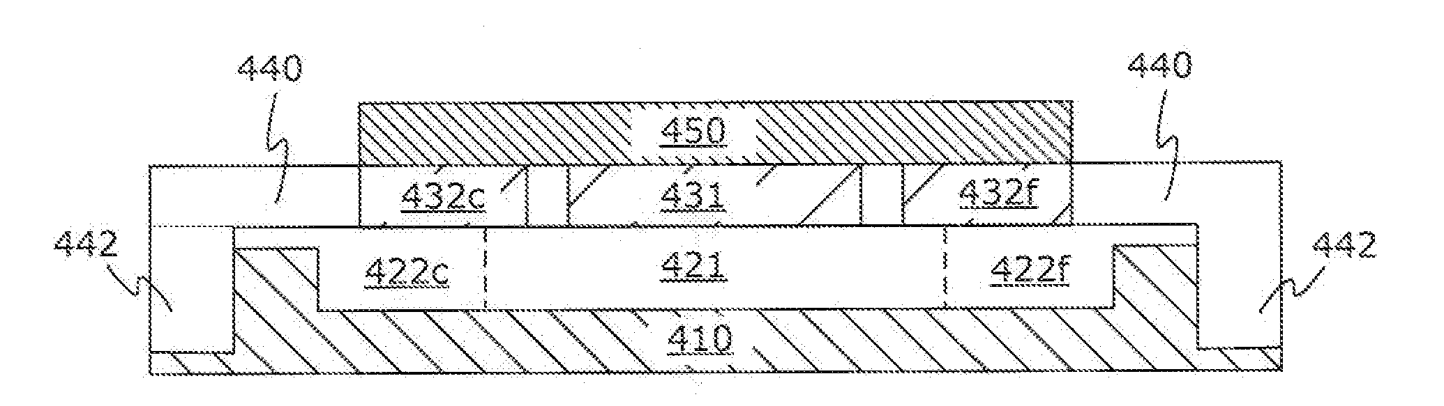
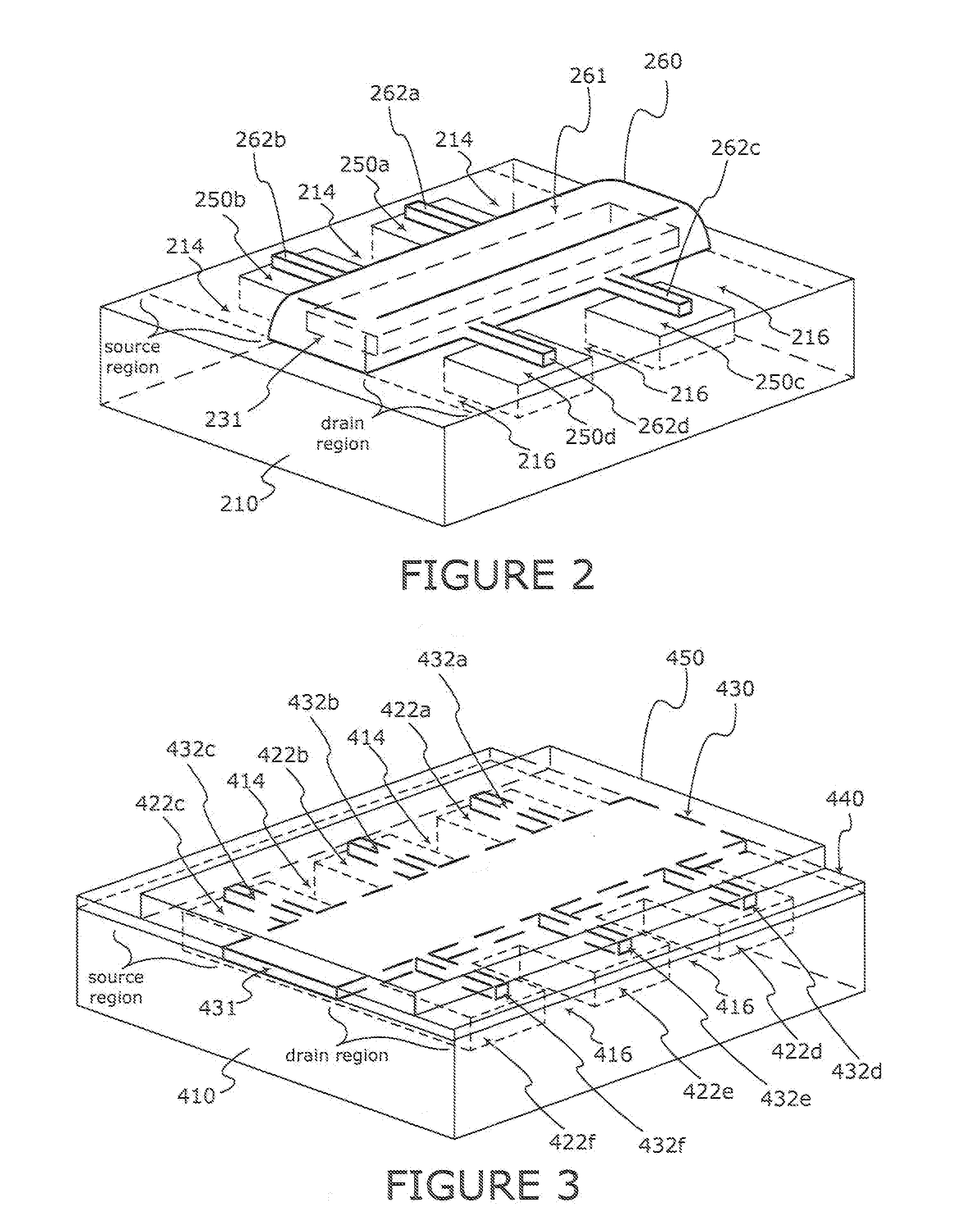
[0020]In particular, embodiments of the present invention describe a semiconductor device utilizing the RESURF effect to optimize the breakdown voltage (BVdss). In an embodiment of the present invention, the semiconductor device comprises a source / drain region haying a plurality of isolation regions interleaved with source / drain extension regions. Agate electrode is formed on the semiconductor device, the gate electrode having gate finger elements formed over the isolation regions. The gate finger elements induce capacitive coupling with the isolation re...


PUM


Abstract

Embodiments of the present invention describe a semiconductor device implementing the reduced-surface-field (RESURF) effect. The semiconductor device comprises a source / drain region having a plurality of isolation regions interleaved with source / drain extension regions. A gate electrode is formed on the semiconductor device, where the gate electrode includes gate finger elements formed over the isolation regions to induce capacitive coupling. The gate finger elements enhance the depletion of the source / drain extension regions, thus inducing a higher breakdown voltage.

Description

BACKGROUND[0001]1. Field[0002]One or more embodiments of the present invention relate to the field of semiconductor devices an more particularly to a transistor with enhanced reduced surface field (RESURF) effect.[0003]2. Discussion of Related Art[0004]Power semiconductor devices, such as high voltage transistors, are designed to support high voltage levels in various applications. In one instance, high voltage transistors are implemented in the peripheral circuitry of semiconductor memory devices such as Flash memory devices. There is constant desire to reduce the size of these memory devices, including the memory cells and the peripheral devices to improve performance. However, downscaling of high voltage transistors is limited by several factors. For example, to maintain a high drain-source breakdown voltage (BVdss), the contact to gate spacing must remain relatively large. Furthermore, the transistor must supply the drive current demanded by circuit operation, which translates t...

Claims


Application Information

Patent Timeline
Patent Type & Authority Applications(United States)
IPC IPC(8): H01L29/78H01L21/336H01L21/28
CPCH01L29/0653H01L29/0847H01L29/402H01L29/4238H01L29/7835H01L29/7833H01L29/6681H01L29/7816H01L29/66575
Inventor SMITH, MICHAEL ANDREW
Owner INTEL NDTM US LLC
Why Eureka
Try Eureka