Image processing circuit

a technology of image processing and circuit, applied in static indicating devices, instruments, cathode-ray tube indicators, etc., can solve the problems of still performing redundant computational processing and potential to be changed more, and achieve the effect of reducing the power consumption of the image processing circui

Inactive Publication Date: 2011-06-23
ROHM CO LTD
View PDF7 Cites 6 Cited by
  • Summary
  • Abstract
  • Description
  • Claims
  • Application Information

AI Technical Summary

Benefits of technology

[0018]In the image processing circuit of the present invention, since tone correction of the input signal is performed based on the created LUT, there is no need for redundant computational processing for input signals that are the same, and the power consumption of the image processing circuit can be reduced.

Problems solved by technology

Although Patent Document 1 discloses a technical idea whereby redundant computational processing is eliminated and power consumption of the image processing circuit is reduced by storing gamma correction results for an input signal as an LUT and gamma-correcting the input signal by referencing the LUT, Patent Document 1 does not disclose a technical idea of using an LUT to store the results of tone correction including contrast adjustment and brightness adjustment, which have the potential to be changed more often by the user.
Interpolation is therefore necessary when the LUT is referenced for tone correction of an input signal, and redundant computational processing is still performed.

Method used


Image

  • Image processing circuit
  • Image processing circuit
  • Image processing circuit

Examples


first embodiment

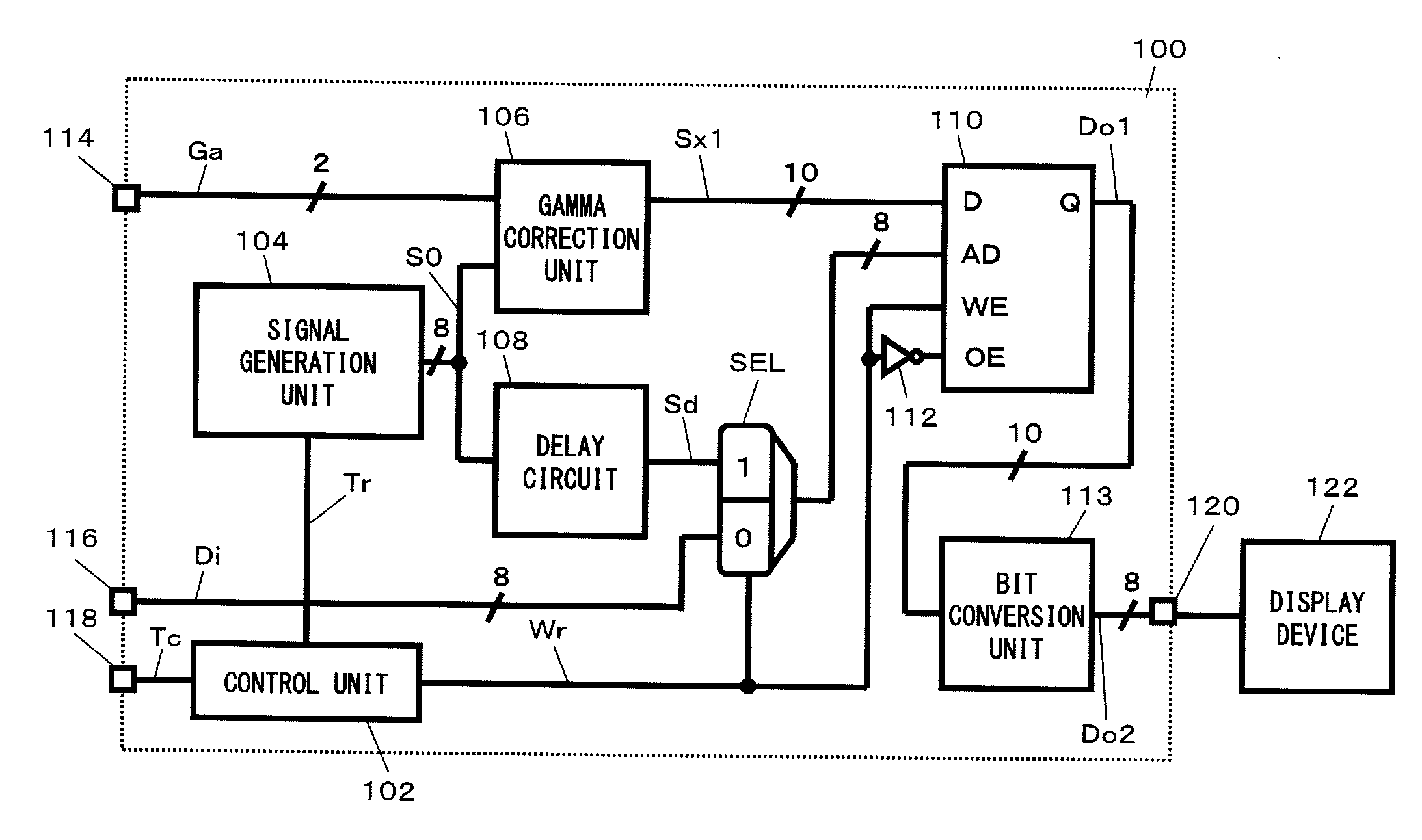
[0031]FIG. 1 shows the image processing circuit according to a first embodiment. The image processing circuit 100 is provided with a control unit 102, a signal generation unit 104, a gamma correction unit 106, a delay circuit 108, a RAM 110, an inverter 112, a bit conversion unit 113, a selector SEL, a gamma setting terminal 114, an input terminal 116, a sync terminal 118, and an output terminal 120. A display device 122 is connected to the output terminal 120.

[0032]The RAM 110 used as a storage device for storing an LUT is provided with a RAM input terminal D, an address terminal AD, a write enable terminal WE, a read enable terminal OE, and a RAM output terminal Q.

[0033]The RAM input terminal D is a terminal for inputting write data to the RAM 110, and the address terminal AD is a terminal for specifying the position (address) of memory to be accessed during data writing or data reading in the RAM 110.

[0034]The write enable terminal WE and the read enable terminal OE are terminals...

second embodiment

[0061]FIG. 6 shows the image processing circuit according to a second embodiment. The image processing circuit 400 differs significantly from the image processing circuit 100 shown in FIG. 1 in that a RAM storage device for storing an LUT is provided independently for each primary-color element of the input signal Di, i.e., for each of R values, G values, and B values. The same reference symbols are used for components which are the same as those in FIG. 1, and no detailed description thereof will be given.

[0062]The image processing circuit 400 is provided with a control unit 402, a signal generating unit 104, a gamma correction unit 106, an R contrast adjustment unit 406, a G contrast adjustment unit 408, a B contrast adjustment unit 410, an R brightness adjustment unit 412, a G brightness adjustment unit 414, a B brightness adjustment unit 416, an R RAM 418, a G RAM 420, a B RAM 422, a delay circuit 108, a selector SEL, and a bit conversion unit 113.

[0063]The image processing circ...


PUM


Abstract

The image processing circuit 400 is provided with R RAM 418, G RAM 420, and B RAM 422. During the vertical blanking interval of a display device 122, tone correction results corresponding to all values which can be inputted as the input signal Di are stored as a lookup table (LUT) in each RAM. When an image is displayed in the display device 122, tone correction of the input signal Di is indirectly performed by referencing the LUT. Redundant computation can thereby be avoided, and power consumption can be reduced.

Description

CROSS-REFERENCE TO RELATED APPLICATIONS[0001]This application is based on Japanese Patent Application No. 2009-285856 filed on Dec. 17, 2009, the contents of which are hereby incorporated by reference.BACKGROUND OF THE INVENTION[0002]1. Field of the Invention[0003]The present invention relates to an image processing circuit.[0004]2. Description of Related Art[0005]Image processing circuits for tone correction of an inputted image signal according to the characteristics of a display device or the preference of a user have been used in the past in cathode ray tube display devices, liquid crystal display devices, and other fields.[0006]Typical methods for tone correction include gamma correction, contrast adjustment, brightness adjustment, and the like, and multiple types of these corrections are usually combined for tone correction of image signals.[0007]FIG. 11 is a block diagram showing a conventional image processing circuit. The image processing circuit 900 is provided with a gamm...

Claims


Application Information

Patent Timeline
Patent Type & Authority Applications(United States)
IPC IPC(8): G09G5/02
CPCG09G3/20G09G2320/0626G09G2320/0673G09G2320/0666G09G2320/066
Inventor YAMASAKI, KOJIICHIHARA, KIYOSHI
Owner ROHM CO LTD
Why Eureka
Try Eureka