Charging circuit and amplifier

a charging circuit and amplifier technology, applied in the direction of electric variable regulation, process and machine control, instruments, etc., can solve the problems of increasing the power consumption of the charge pump circuit, the time needed for boosting the charge voltage of the capacitor gets longer than a time,

Active Publication Date: 2011-06-23
SEMICON COMPONENTS IND LLC
View PDF4 Cites 49 Cited by
  • Summary
  • Abstract
  • Description
  • Claims
  • Application Information

AI Technical Summary

Benefits of technology

[0007]An charging circuit according to an aspect of the present invention, comprises: a charge pump circuit configured to generate a boosted vol

Problems solved by technology

When the LPF is provided to eliminate noises included in the boosted voltage, as described above, however, a time needed for boosting the charge voltage of the capacitor gets longer than a time nee

Method used


Image

  • Charging circuit and amplifier
  • Charging circuit and amplifier
  • Charging circuit and amplifier

Examples


Embodiment Construction

[0016]At least the following details will become apparent from descriptions of this specification and of the accompanying drawings.

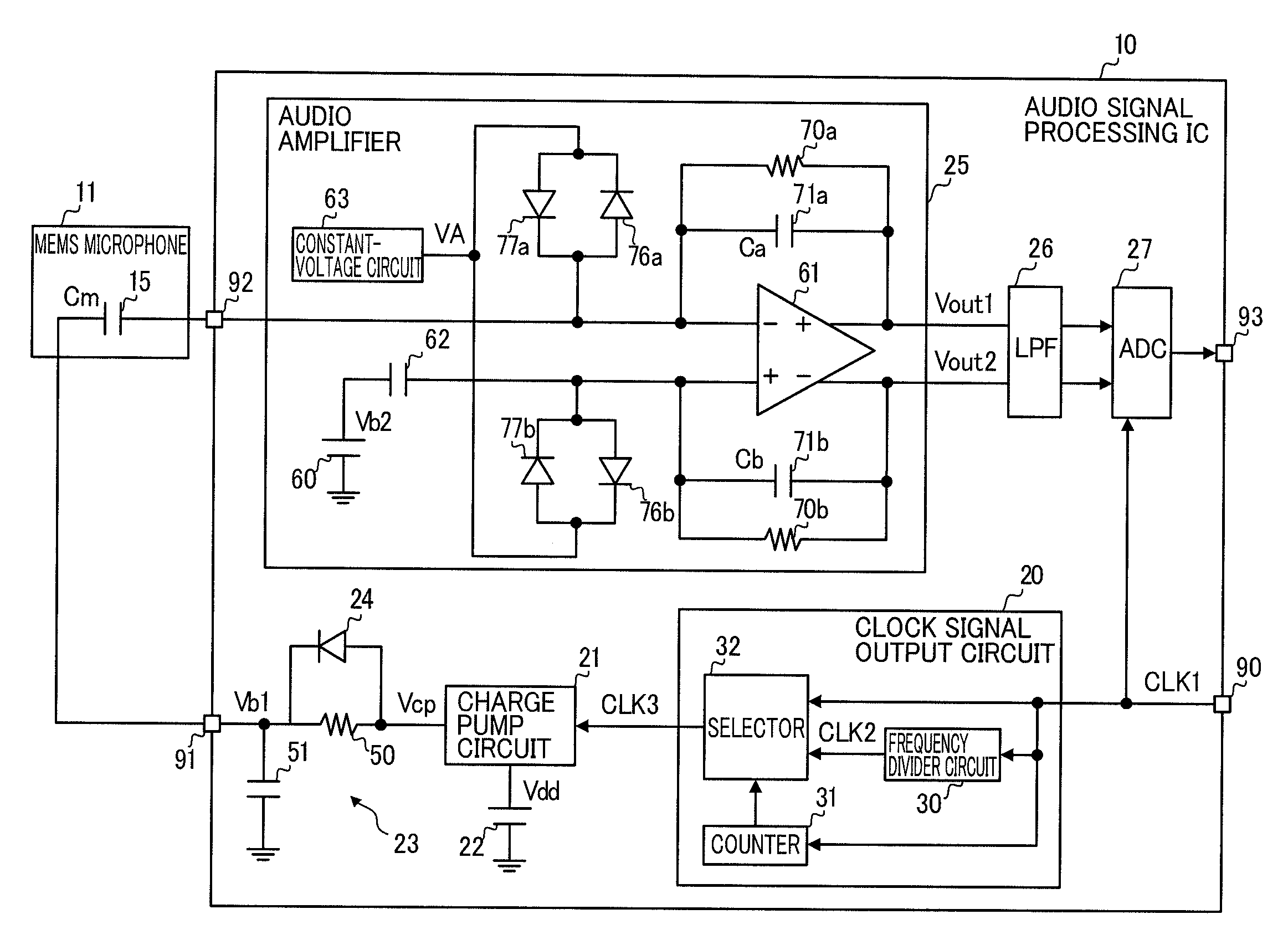
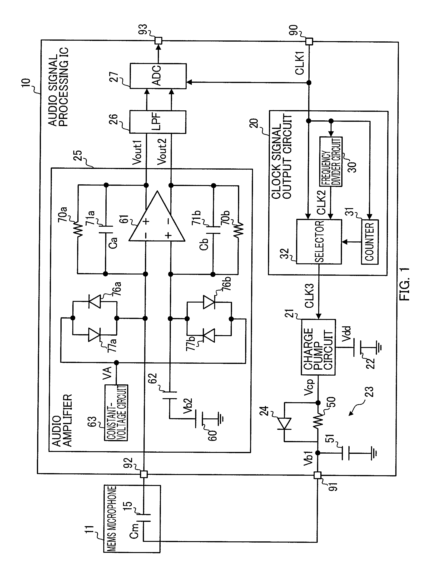
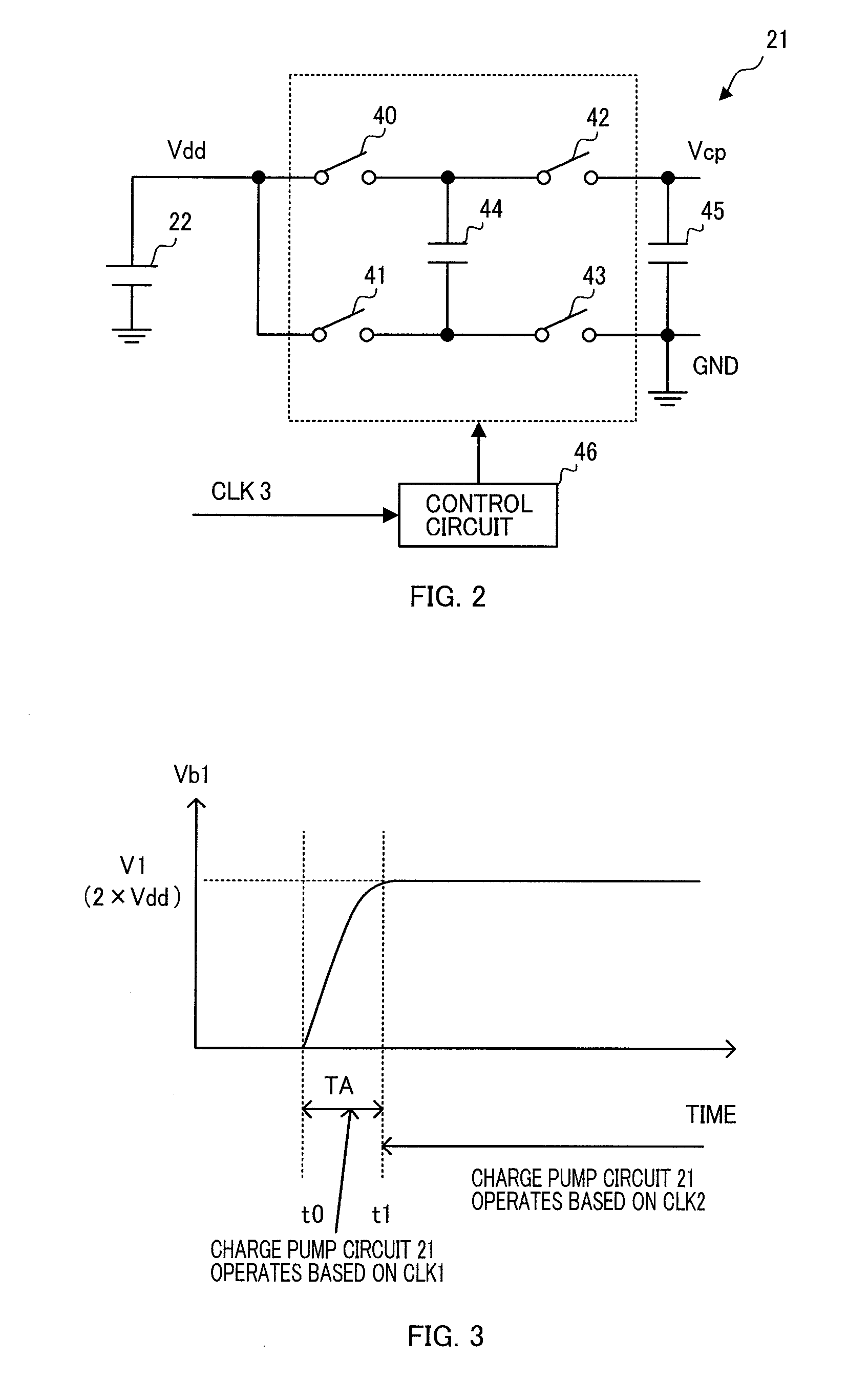
[0017]FIG. 1 depicts a configuration of an audio signal processing IC (Integrated Circuit) 10 of one embodiment of the present invention. The audio signal processing IC 10 is, for example, a circuit that amplifies and digitizes an audio signal detected by an MEMS (Micro Electromechanical System) microphone 11. The audio signal processing IC 10 includes a clock signal output circuit 20, a charge pump circuit 21, a power supply circuit 22, LPFs 23 and 26, a diode 24, an audio amplifier 25, an ADC (Analog-to-Digital Converter) 27, and terminals 90 to 93. The clock signal output circuit 20, the charge pump circuit 21, and the LPF 23 correspond to a charging circuit.

[0018]The MEMS microphone 11 connected between the terminal 91 and the terminal 92 is a capacitor microphone that generates a signal in accordance with an audio, and includes a capacitor 15 whose ...


PUM


Abstract

A charging circuit comprising:
    • a charge-pump circuit configured to generates a boosted voltage obtained by boosting an input voltage at each time interval shorter in accordance with an increase of a frequency of an input clock signal;
    • an integrating circuit configured to integrate the boosted voltage to apply the integrated boosted voltage to a capacitor; and
    • a clock signal output circuit configured to output a second clock signal higher in frequency than a first clock signal to the charge-pump circuit as the clock signal, and thereafter output the first clock signal to the charge-pump circuit as the clock signal, in order that a charge voltage of the capacitor reaches a predetermined voltage level in a time shorter than a time in which the charge voltage of the capacitor reaches the predetermined voltage level when the first clock signal is input to the charge-pump circuit as the clock signal.

Description

CROSS-REFERENCE TO RELATED APPLICATION[0001]This application claims the benefit of priority to Japanese Patent Application No. 2009-287598, filed Dec. 18, 2009, of which full contents are incorporated herein by reference.BACKGROUND OF THE INVENTION[0002]1. Field of the Invention[0003]The present invention relates to a charging circuit and an amplifier.[0004]2. Description of the Related Art[0005]A charge pump circuit is known as a circuit that applies a boosted voltage generated by boosting an input voltage to a load, such as a capacitor (see, e.g., Japanese Laid-Open Patent Publication No. 2006-50833). Because the charge pump circuit usually generates the boosted voltage in synchronization with an input clock signal, noises are included in the boosted voltage. To eliminate such noises, for example, an LPF (Low-pass Filter) may be placed between the charge pump circuit and the capacitor as a load.[0006]Capacitive loads driven by the charge pump circuit include, for example, a capaci...

Claims


Application Information

Patent Timeline
IPC IPC(8): H04R3/00G05F1/10
CPCH02M3/07H03F3/187H03F3/45475H03F2203/45571H03F2203/45526H03F2203/45568H03F2200/03
Inventor ONISHI, AKINOBU
Owner SEMICON COMPONENTS IND LLC
Why Eureka
Try Eureka