Circuit substrate and manufacturing method thereof

Inactive Publication Date: 2011-06-30
SUBTRON TECH
View PDF10 Cites 15 Cited by
  • Summary
  • Abstract
  • Description
  • Claims
  • Application Information

AI Technical Summary

Benefits of technology

[0008]The invention is directed to a circuit substrate and a manufacturing method thereof, which can reduc

Problems solved by technology

Since the substrate with a certain thickness hast to be provided to serve as the support carrier of a copper foil layer according to the conventional technique, if a material of the substrate is a metal material, material cost thereof is relatively high, so that manufacturing cost of the multi-layer circuit board is increased.
Moreover, a large amount of adhesive is required for fixing the copper foil laye

Method used


Image

  • Circuit substrate and manufacturing method thereof
  • Circuit substrate and manufacturing method thereof
  • Circuit substrate and manufacturing method thereof

Examples


Example

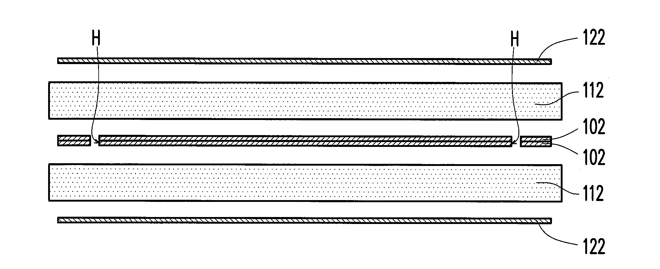
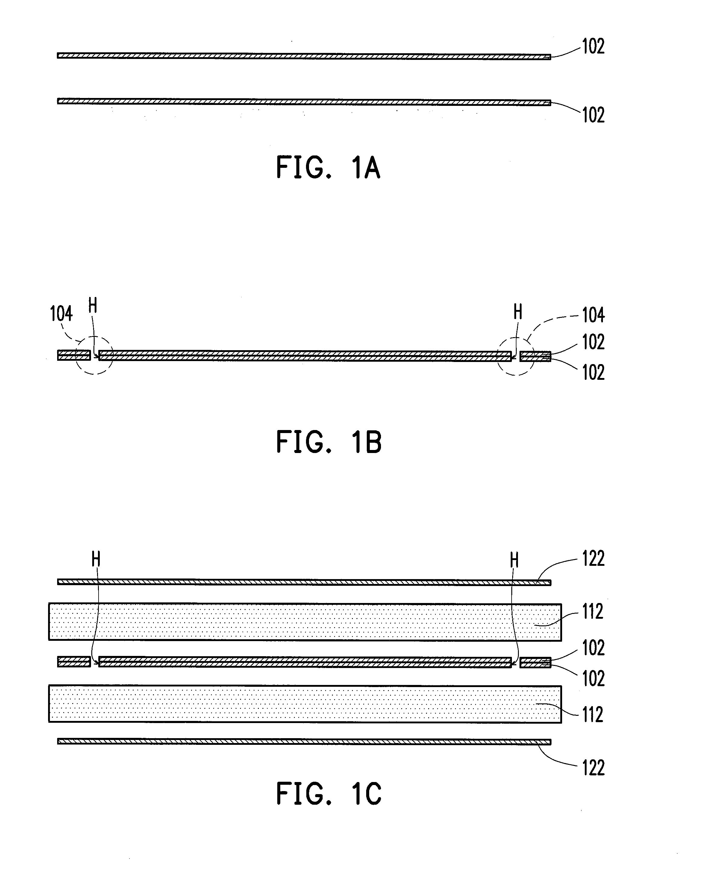
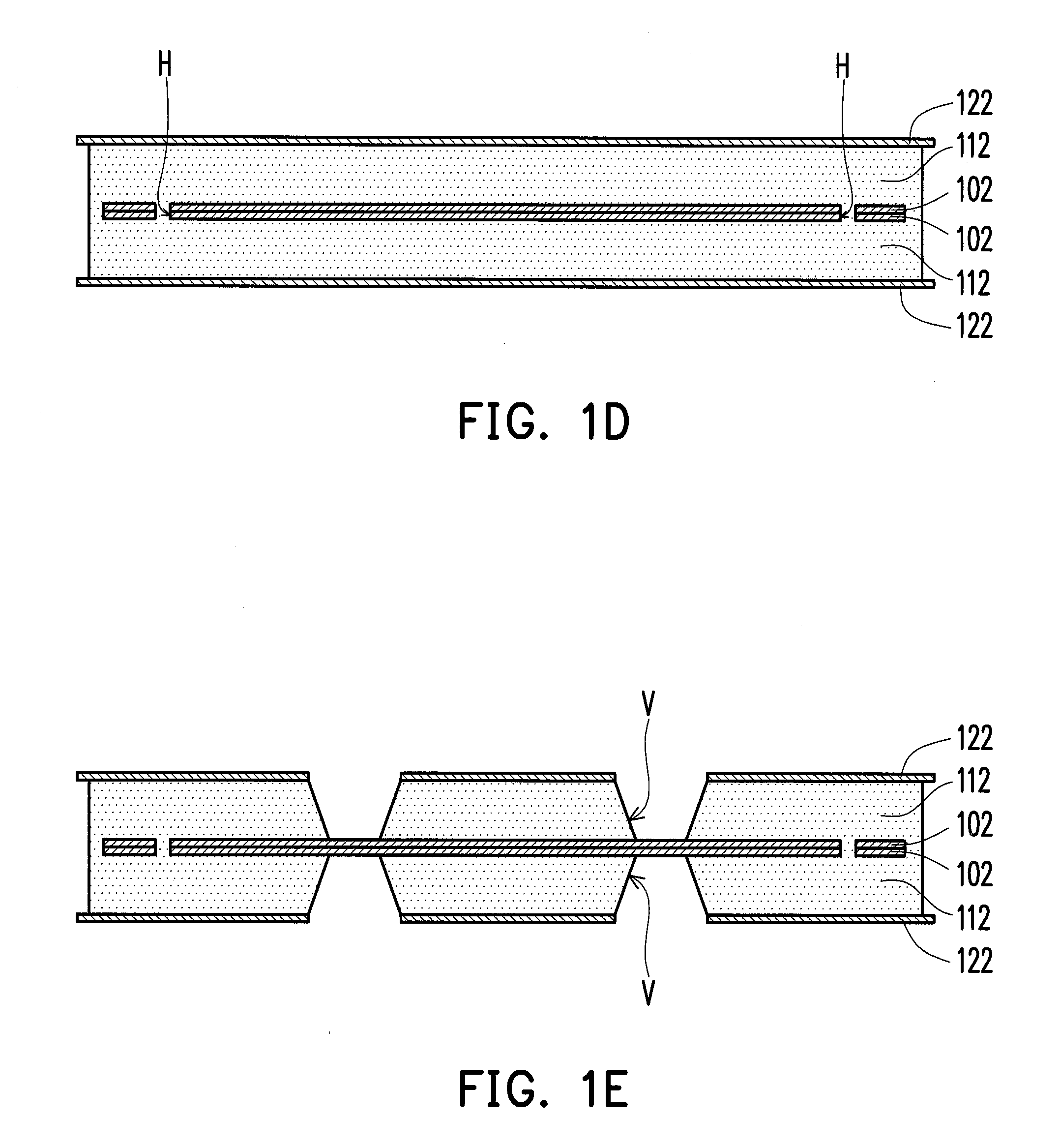
[0035]FIG. 1A to FIG. 1H are cross-sectional views illustrating a manufacturing method of a circuit substrate according to an embodiment of the invention. Referring to FIG. 1A and FIG. 1B, the manufacturing method of the circuit substrate can be described as follow. First, two metal layers 102 are provided, where the two metal layers 102 are, for example, copper foils or other metal foils, and peripheries of the two metal layers 102 are bonded to form a sealed area 104. In the present embodiment, a method of bonding the peripheries of the two metal layers 102 includes welding or spot welding, so that the two metal layers 102 are temporarily bonded to avoid reagents used in follow-up processes from infiltrating there between. Certainly, besides the welding or spot welding, an adhesive can also be used to temporarily bond the peripheries of the two metal layers 102, where a material of the adhesive includes cyanoacrylate ester or polypropylene resin, or other adhesives. It should be n...


PUM

PropertyMeasurementUnit
Thicknessaaaaaaaaaa
Electrical conductoraaaaaaaaaa
Areaaaaaaaaaaa

Abstract

A manufacturing method of a circuit substrate includes the following steps. The peripheries of two metal layers are bonded to form a sealed area. At least a through hole passing through the sealed area is formed. Two insulating layers are formed on the two metal layers. Two conductive layers are formed on the two insulating layers. The two insulating layers and the two conductive layers are laminated to the two metal layers bonded to each other, wherein the metal layers are embedded between the two insulating layers, and the two insulating layers fill into the through hole. The sealed area of the two metal layers is separated to form two separated circuit substrates. Therefore, the thinner substrate can be operated in the following steps, such as patterning process or plating process. In addition, the method may be extended to manufacture the circuit substrate with odd-numbered layer or even-numbered layer.

Description

CROSS-REFERENCE TO RELATED APPLICATION[0001]This application claims the priority benefit of Taiwan application serial no. 98145638, filed on Dec. 29, 2009, Taiwan application serial no. 99112313, filed on Apr. 20, 2010, and Taiwan application serial no. 99141954, filed on Dec. 2, 2010. The entirety of each of the above-mentioned patent applications is hereby incorporated by reference herein and made a part of specification.BACKGROUND[0002]1. Field of the Invention[0003]The invention relates to a circuit substrate and a manufacturing method thereof. Particularly, the invention relates to a coreless circuit substrate and a manufacturing method thereof.[0004]2. Description of Related Art[0005]In a current semiconductor manufacturing process, a chip package carrier is one of commonly used packaging components. The chip package carrier is, for example, a multi-layer circuit board, which is mainly formed by alternately stacking multiple circuit layers and a multiple dielectric layers, whe...

Claims


Application Information

Patent Timeline
IPC IPC(8): H05K3/00
CPCH05K3/0097H05K3/427H05K2201/09509Y10T29/49124H05K2203/0228H05K2203/1536H05K2201/096Y10T29/49126Y10T29/49156
Inventor CHUANG, CHIH-HONGHUANG, TZU-WEI
Owner SUBTRON TECH
Why Eureka
Try Eureka