Method of manufacturing electronic cards

a manufacturing method and electronic card technology, applied in the field of manufacturing complex electronic cards, can solve the problems of major drawbacks for those skilled in the art specialised in manufacturing finished electronic cards or inlets

Inactive Publication Date: 2011-06-30
NAGRAVISION SA
View PDF4 Cites 9 Cited by
  • Summary
  • Abstract
  • Description
  • Claims
  • Application Information

AI Technical Summary

Benefits of technology

[0020]It will be noted that, in a variant, the protective film has an adhesive surface that holds it in place and also, in a subsequent step of depositing a filler material at least partially covering the electronic connection, prevents said filler material from infiltrating underneath the protective film and thus flowi

Problems solved by technology

However, the manufacturing method presents a problem in relation to the sequence of steps, in particular the fact that the electrical connection between the visible electronic element and the internal electronic unit is achieved once the electronic element has been inserted in a window in an external insulating layer of the card being manufactured and the adhesive protective layer is in place.
This sequence of steps raises a practical problem given that card m

Method used


Image

  • Method of manufacturing electronic cards
  • Method of manufacturing electronic cards
  • Method of manufacturing electronic cards

Examples


Embodiment Construction

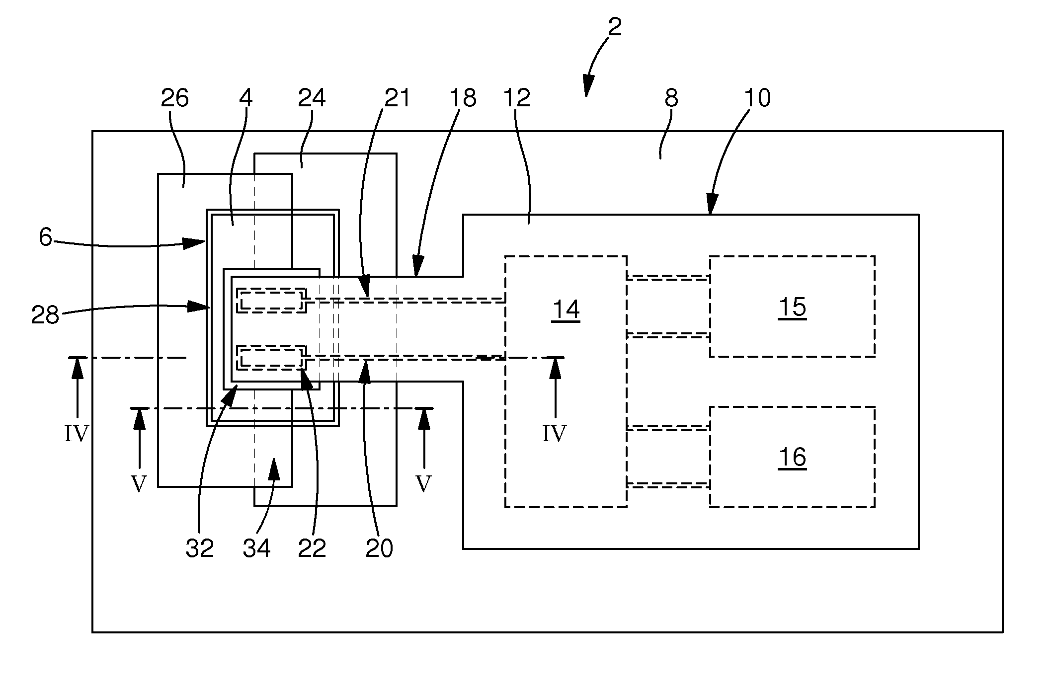
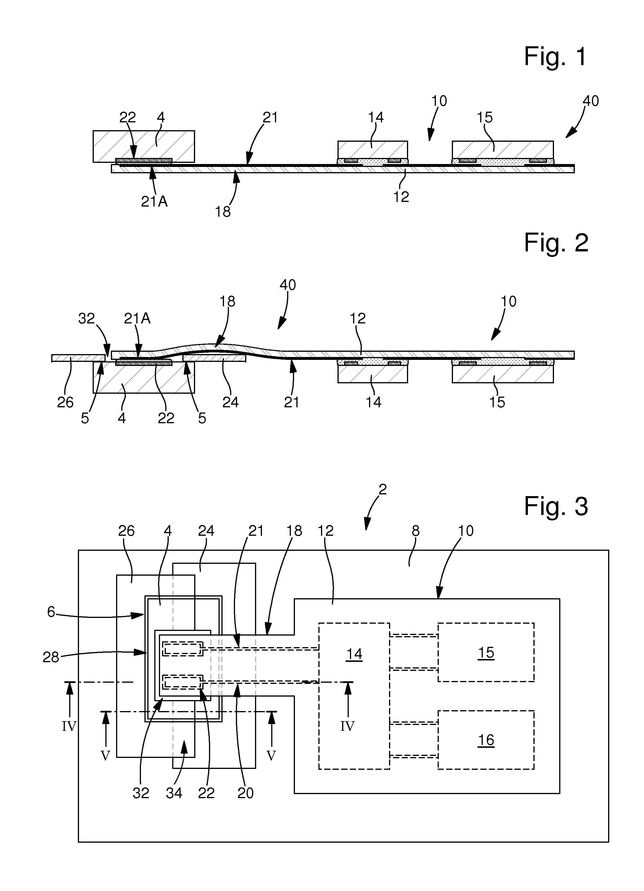
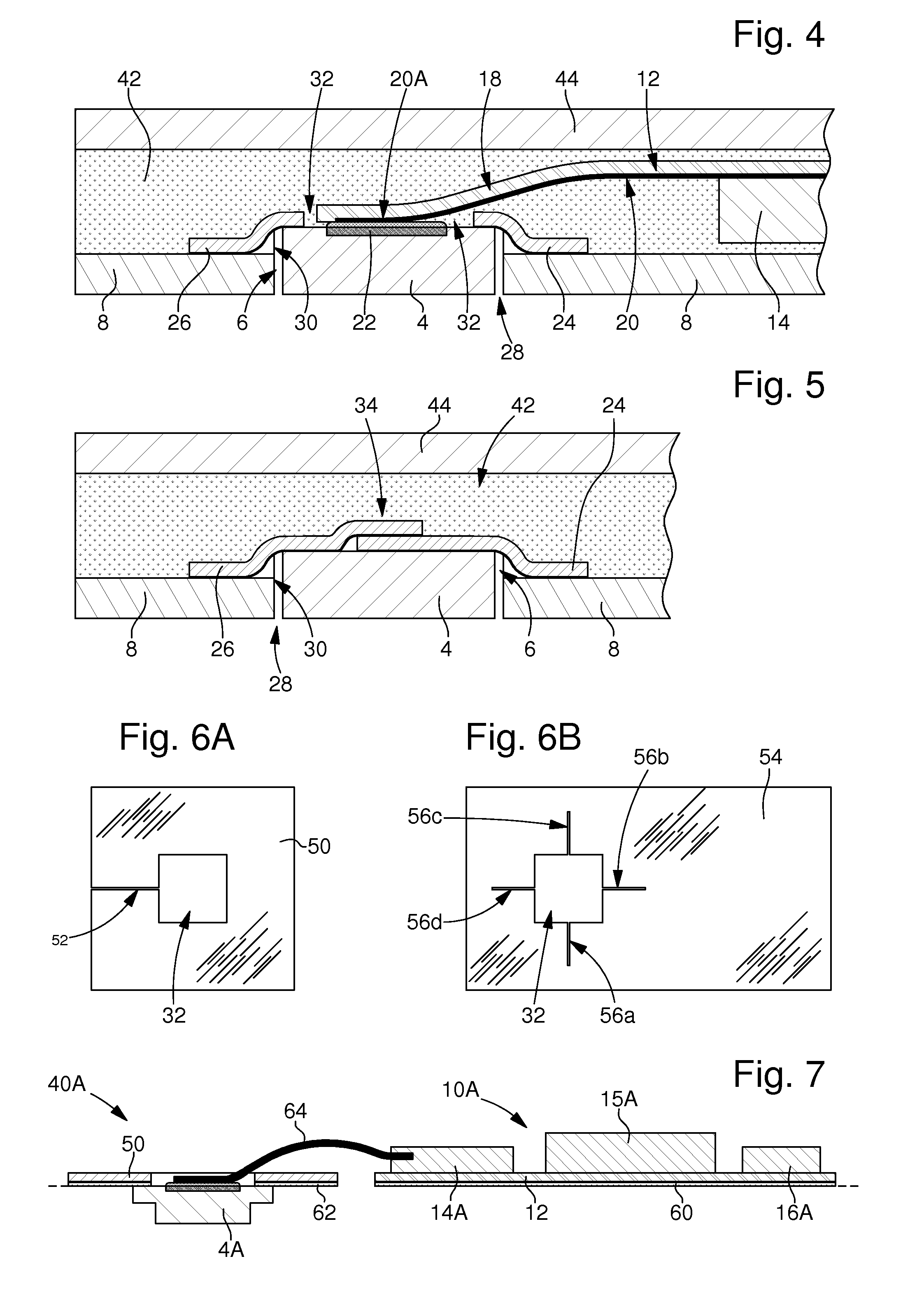
[0036]With reference to FIGS. 1 to 5, a first implementation mode of an electronic card manufacturing method according to the invention will be described below.

[0037]In a preliminary step of this card manufacturing method, a first electronic unit 4 is assembled to a second electronic unit 10 to form electronic assembly or device 40. Electronic unit 10 is formed of a PCB type support 12 at the surface of which various components 14, 15 and 16 are arranged. These electronic circuits can be formed of any type of component and may have various functions. Component 14 can for example be a micro-processor, component 15 a display and component 16 a battery. It will be noted that the second electronic unit 10 can also, in a variant, form a battery or, in another variant, form an antenna. It will also be noted that the first electronic unit can be formed by a single external electric contact pad connected to an internal electronic unit of the card.

[0038]PCB 12 can be rigid or flexible. This ...


PUM

PropertyMeasurementUnit
Fractionaaaaaaaaaa
Pressureaaaaaaaaaa
Shapeaaaaaaaaaa

Abstract

The present invention concerns a method of manufacturing complex electronic cards each including an electronic device or assembly (40) formed of a first electronic unit (4) at least partially arranged in a window in a solid bottom layer of the card and a second electronic unit (10), incorporated in the body of the card, at least partially formed by a resin provided on the solid bottom layer. In order to prevent the resin from flowing into a slit between the lateral wall of the window and the second unit inserted therein, a protective film is arranged to cover the edge of the rear face of the first unit and a zone peripheral to the aperture in the solid layer. According to the invention, the electronic device or assembly (40) is first formed and then placed on the bottom solid layer. The protective film is arranged between the two units after or when the electronic device or assembly is formed. Therefore according to the invention the protective film is formed, for example, of several parts (24, 26) having respective profiles that define an aperture into which the electrical connection (18) between the two electronic units (4, 10) passes. In another embodiment, the protective film is formed of a single part having at least one slit starting from an aperture (32) made in said part and provided to allow the electrical connection to pass therethrough. In another embodiment, the protective film has flaps at the edge of the aperture and is assembled to the solid bottom layer prior to addition of the electronic device or assembly.

Description

[0001]This application claims priority from European Patent Application No. 09180782.6 filed Dec. 28, 2009, the entire disclosure of which is incorporated herein by reference.FIELD OF THE INVENTION[0002]The present invention concerns a method of manufacturing complex electronic cards each including a first electronic unit, at least partially arranged in a window in a solid layer of the card, and a second electronic unit electrically connected to the first electronic unit and incorporated in an internal layer formed by a filler material which covers at least one of the surfaces of said second electronic unit. In particular, the filler material is a resin, provided in a non solid state during the manufacturing process or a resin provided in the form of at least partially melted hot melt sheets, so as form an internal layer of the card. It will be noted that the internal layer formed by the filler material can contain other solid structures or elements, in particular positioning or fil...

Claims


Application Information

Patent Timeline
IPC IPC(8): H05K3/10
CPCG06K19/072G06K19/077Y10T29/49126Y10T29/49165Y10T29/49155Y10T29/4913G06K19/0772
Inventor DROZ, FRANCOIS
Owner NAGRAVISION SA
Why Eureka
Try Eureka