Solid-state image pickup apparatus and image pickup system

a solid-state image and pickup apparatus technology, applied in the field of backside-illumination solid-state image pickup apparatus, can solve problems such as image white defects

Active Publication Date: 2011-06-30
CANON KK
View PDF5 Cites 135 Cited by
  • Summary
  • Abstract
  • Description
  • Claims
  • Application Information

AI Technical Summary

Benefits of technology

[0007]The present invention provides an apparatus in which a first substrate and a second substrate are placed upon each other, the first substrate being where a photoelectric conversion element and a gate electrode for transferring an electric charge from the photoelectric conversion element are disposed, the second substrate being where a peripheral circuit portion for reading out a signal based on the electric charge generated at the photoelectric conversion element is disposed, wherein the second substrate is provided with a high-melting-metal compound layer, and the first substrate is not provided with a high-melting-metal compound layer.

Problems solved by technology

In addition, for example, a white defect may occur in an image due to leakage current generated as a result of contamination of the photoelectric conversion element by the high-melting metal.

Method used


Image

  • Solid-state image pickup apparatus and image pickup system
  • Solid-state image pickup apparatus and image pickup system
  • Solid-state image pickup apparatus and image pickup system

Examples


first embodiment

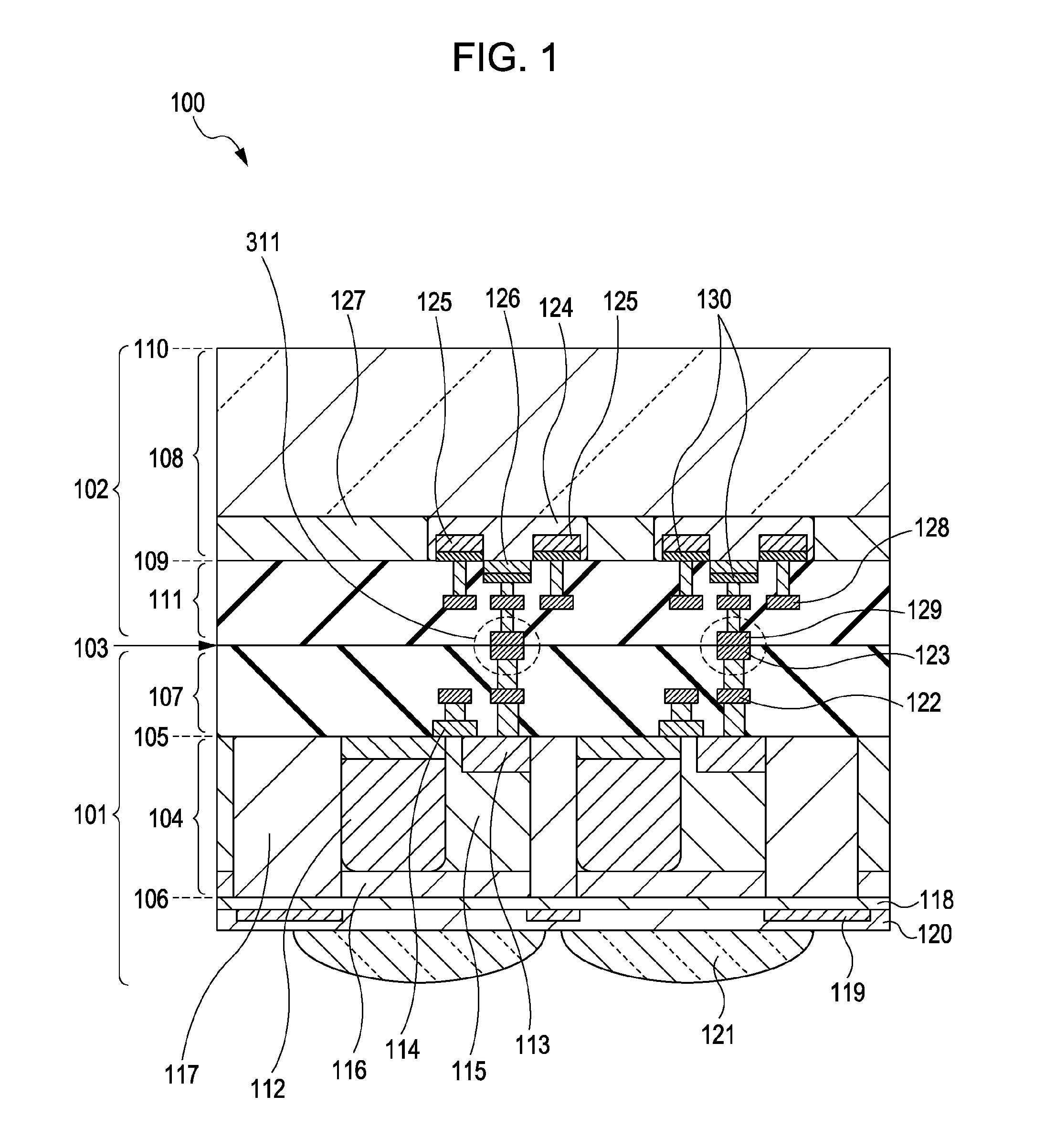
[0024]A first embodiment of the present invention will be described with reference to FIGS. 1 and 12.

[0025]First, an exemplary circuit of a solid-state image pickup apparatus according to the first embodiment will be described with reference to FIG. 12. A solid-state image pickup apparatus 300 shown in FIG. 12 includes a pixel portion 301, in which a plurality of photoelectric conversion elements are arranged, and a peripheral circuit portion 302, provided with a control circuit for performing a driving operation for reading out a signal from the pixel portion 301 and with a signal processing circuit that processes the readout signal.

[0026]In the pixel portion 301, a plurality of photoelectric conversion elements 303, transfer transistors 304, amplification transistors 306, and reset transistors 307 are disposed. A structure including at least one photoelectric conversion element 303 is defined as a pixel. One pixel in the embodiment includes the photoelectric conversion element 303...

second embodiment

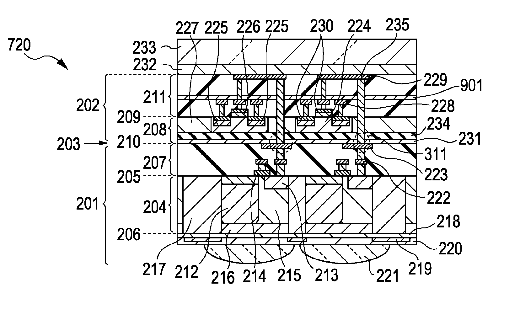
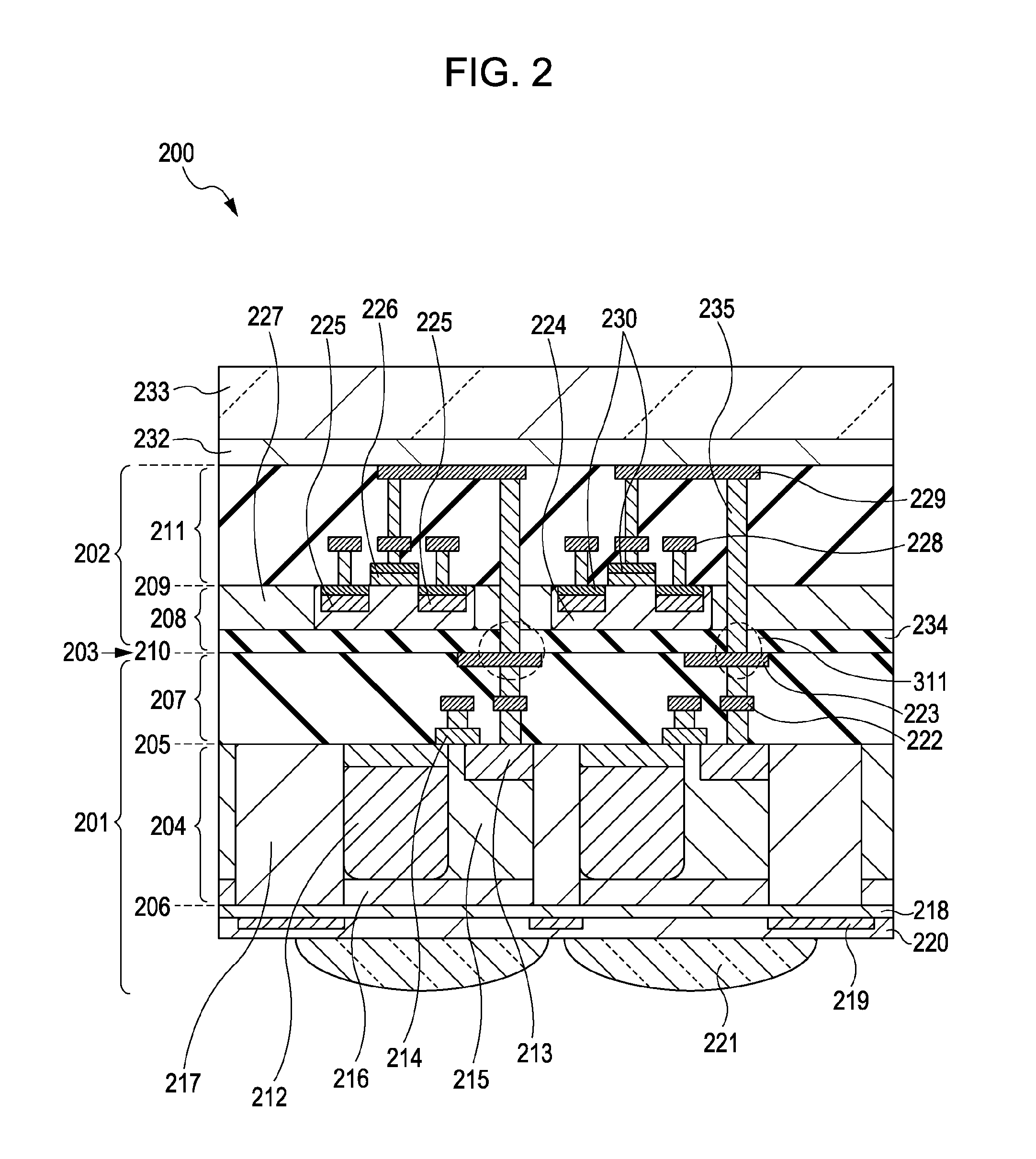
[0039]A solid-state image pickup apparatus according to this embodiment will be described with reference to FIG. 2. The solid-state image pickup apparatus according to the embodiment is similar to the solid-state image pickup apparatus according to the first embodiment in that its circuits are equivalent to those shown in FIG. 12, and differs therefrom in its chip stacking structure. A description of the circuits will hereunder be omitted. The structure shown in FIG. 2 will hereunder be described.

[0040]FIG. 2 is a sectional view of a solid-state image pickup apparatus 200 corresponding to the circuits shown in FIG. 12. FIG. 2 is a sectional view for two pixels in correspondence with the photoelectric conversion elements 303, the transfer transistors 304, and the amplification transistors 306 shown in FIG. 12, and does not show the other portions.

[0041]FIG. 2 shows a first chip 201, a second chip 202, and a bonding surface 203 of the first chip and the second chip. The first chip 201...

third embodiment

[0048]A solid-state image pickup apparatus according to this embodiment will be described with reference to FIG. 3. The solid-state image pickup apparatus according to the embodiment corresponds to the solid-state image pickup apparatus 100 according to the first embodiment, and differs therefrom in that it includes a diffusion prevention film. The structure shown in FIG. 3 will hereunder be described. The structural features that are equivalent to those of the first embodiment will not be described.

[0049]In a solid-state image pickup apparatus 400 shown in FIG. 3, a diffusion prevention film 131 is disposed between a first chip 101 and a second chip 102. By providing such a diffusion prevention film 131, it is possible to suppress diffusion of a high-melting metal of a high-melting-metal compound layer disposed at the second chip into multilayer wiring structures 111 and 107 and mixture of the high-melting metal into a semiconductor region constituting an FD region and a photoelect...


PUM


Abstract

An apparatus according to the present invention in which a first substrate including a photoelectric conversion element and a gate electrode of a transistor, and a second substrate including a peripheral circuit portion are placed upon each other. The first substrate does not include a high-melting-metal compound layer, and the second substrate includes a high-melting-metal compound layer.

Description

TECHNICAL FIELD[0001]The present invention relates to a backside-illumination solid-state image pickup apparatus.BACKGROUND ART[0002]Recent higher-speed solid-state image pickup apparatuses have caused the proposal of a structure in which a semiconductor compound layer is provided at a transistor.[0003]Japanese Patent Laid-Open No. 2001-111022 discusses a solid-state image pickup apparatus in which a high-melting-metal semiconductor compound layer is not provided on a photodetector of a photoelectric converting section, and a high-melting-metal semiconductor compound layer is provided at a peripheral circuit portion.[0004]Japanese Patent Laid-Open No. 2009-170448 discusses a backside-illumination solid-state image pickup apparatus in which, in order to increase sensitivity of a photoelectric conversion element, a substrate including a pixel portion provided with the photoelectric conversion element and a signal-readout circuit, and a substrate including a peripheral circuit for proc...

Claims


Application Information

Patent Timeline
Patent Type & Authority Applications(United States)
IPC IPC(8): H01L27/146H01L31/0224
CPCH01L27/14632H01L27/14636H01L27/14687H01L27/1464H04N5/374H04N5/3742H01L31/02H01L27/1469H01L2224/80895H01L2224/80896H01L27/14612H01L27/14634H01L2224/8034H04N25/767H04N25/76H01L27/146H04N25/00H01L27/14623H01L27/14627H01L27/1463H01L27/14645
Inventor ENDO, NOBUYUKIITANO, TETSUYAYAMAZAKIWATANABE, KYOUHEIICHIKAWA, TAKESHI
Owner CANON KK
Why Eureka
Try Eureka