Semiconductor device and manufacturing method of semiconductor device

Inactive Publication Date: 2011-06-30
RENESAS ELECTRONICS CORP
View PDF3 Cites 21 Cited by
  • Summary
  • Abstract
  • Description
  • Claims
  • Application Information

AI Technical Summary

Benefits of technology

[0013]According to the embodiment, the end of the fixed layer of the magnetoresistive element of the semiconductor device provided is pro

Problems solved by technology

In this case, the magnetic field leaking from the fixed layer become noise, and may possibly cause the free layer to be magnetized in the wrong direction.
Thus, the magnetoresistive effect element reduces the possibility that the magnetic field leaking from the fixed layer will become noise and that the free layer will be magnetized in the wrong direction.
Howe

Method used


Image

  • Semiconductor device and manufacturing method of semiconductor device
  • Semiconductor device and manufacturing method of semiconductor device
  • Semiconductor device and manufacturing method of semiconductor device

Examples


Example

First Embodiment

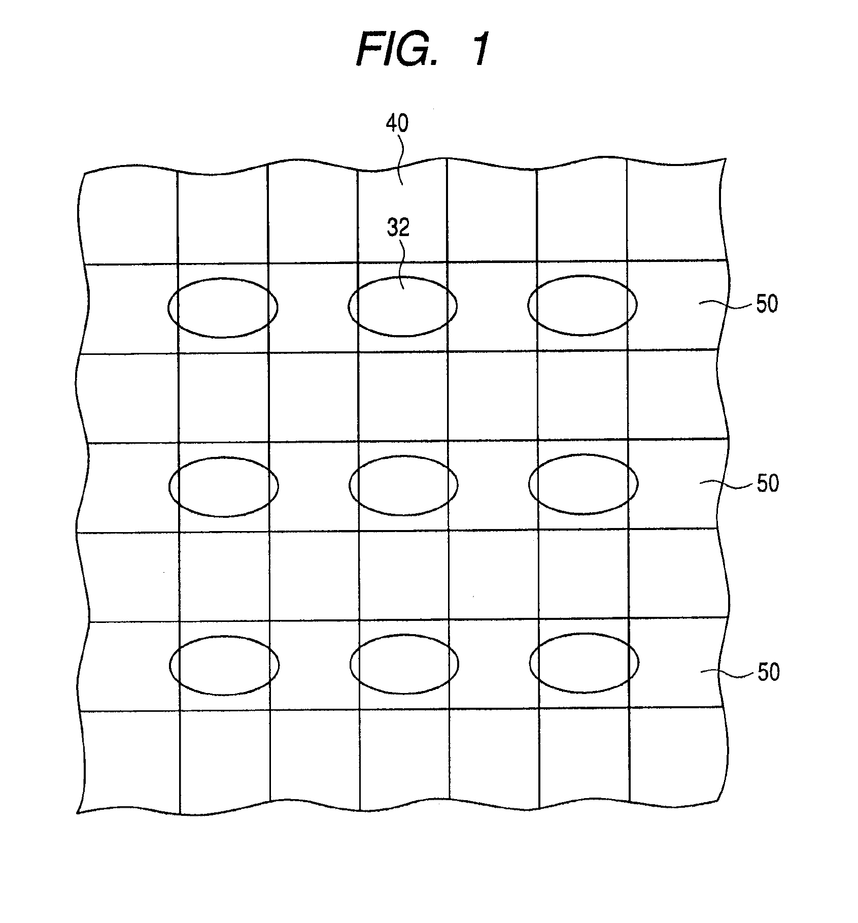
[0088]FIG. 1 is an exemplary plan view showing a semiconductor device 200 according to a first embodiment of the invention. As shown in FIG. 1, a semiconductor substrate 100 is provided with bit lines 40 extending in one direction, digit lines 50 positioned below the bit lines 40 and formed to intersect the respective bit lines 40, and magnetoresistive elements 32, each positioned between the digit line 50 and the bit line 40, and formed in a region where the digit line 50 and the bit line 40 intersect.

[0089]The bit lines 40 extend in one direction and are formed spaced apart from each other. The digit lines 50 extend in the direction of arrangement of the bit lines 40, and are formed spaced apart from each other in the direction of extension of the bit line 40. Each magnetoresistive element 32 is provided in the corresponding region where the digit line 50 and the bit line 40 intersect.

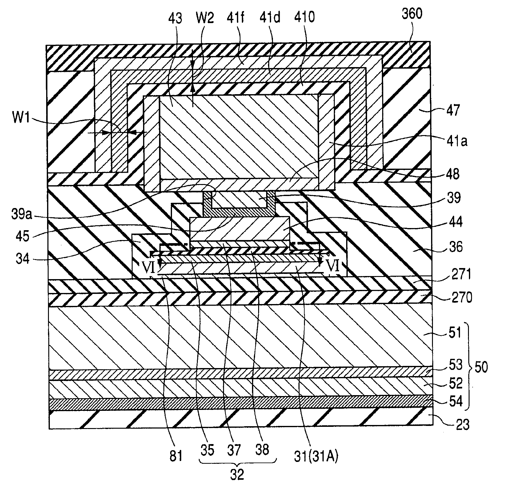
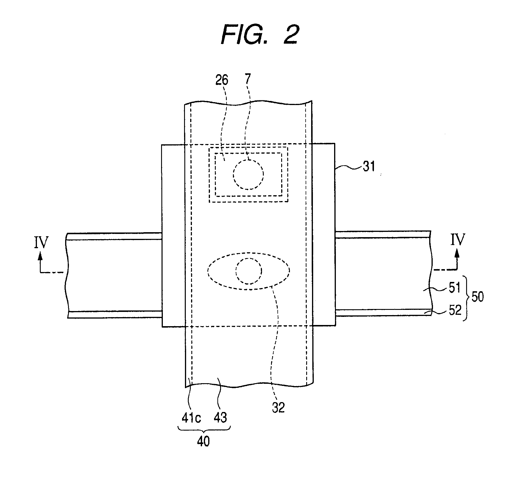
[0090]FIG. 2 is a plan view showing the magnetoresistive element 32 and its surro...

Example

Second Embodiment

[0208]The semiconductor device 200 according to a second embodiment has the substantially same structure as that of the semiconductor device 200 of the first embodiment. The second embodiment slightly differs from the first embodiment in the structure of the magnetoresistive element 32. Specifically, by comparing FIG. 43 with FIG. 28, a magnetoresistive element 32 of the second embodiment includes a second upper electrode 94 in addition to the first upper electrode 44. The magnetoresistive element 32 of the first embodiment has only the single-layered upper electrode, namely, the first upper electrode 44, but has the two-layered lower electrode, namely, the first lower electrode 31 and the second lower electrode 81. The magnetoresistive element 32 of the second embodiment, however, has two-layered structure in each of the upper electrode and the lower electrode. Thus, also the upper electrode may be comprised of two-layered structure, like the lower electrode. The s...

Example

Third Embodiment

[0226]A semiconductor device 200 of the third embodiment includes substantially the same structure as that of the semiconductor device 200 of the second embodiment, but includes a few differences of the magnetoresistive element 32 from that of the second embodiment. Specifically, by comparing FIG. 51 with FIG. 43, the magnetoresistive element 32 of the third embodiment includes a third upper electrode 95 in addition to the first upper electrode 44 and the second upper electrode 94. The semiconductor device 200 of this embodiment includes a third lower electrode 82, in addition to the first lower electrode 31 and the second lower electrode 81. In the magnetoresistive element 32 of the second embodiment, the upper electrode has a two-layered structure of the first upper electrode 44 and the second upper electrode 94, and the lower electrode has a two-layered structure of the first lower electrode 31 and the second lower electrode 81. In the magnetoresistive element 32 ...


PUM


Abstract

A semiconductor device is provided which can further suppress the leakage of a magnetic field in a magnetoresistive element, and which can further improve the performance of the semiconductor device. A semiconductor device includes a semiconductor substrate, a lower electrode, a magnetoresistive element, an upper electrode, and a protective film. The lower electrode is formed over a main surface of the semiconductor substrate. The magnetoresistive element includes a fixed layer, a tunneling insulating film, and a free layer. The upper electrode is disposed over the other main surface opposite to one main surface of the free layer opposed to the tunneling insulating film. The protective film covers the sides intersecting the main surfaces of the lower electrode, the fixed layer, the tunneling insulating film, the free layer, and the upper electrode. The fixed layer included in the magnetoresistive element is a layer which is disposed over one main surface of the lower electrode, and whose magnetization direction is fixed. The tunneling insulating film is disposed over the other main surface opposite to one main surface of the fixed layer opposed to the lower electrode. The free layer is a layer which is disposed over the other main surface opposite to one main surface of the tunneling insulating film opposed to the fixed layer, and whose magnetization direction is variable. The width of the upper electrode is smaller than that of each of the lower electrode and the fixed layer in the direction intersecting the lamination direction of the lower electrode, the fixed layer 35, the tunneling insulating film 38, the free layer, and the upper electrode.

Description

CROSS-REFERENCE TO RELATED APPLICATIONS[0001]The disclosure of Japanese Patent Application No. 2009-294920 filed on Dec. 25, 2009 including the specification, drawings and abstract is incorporated herein by reference in its entirety.BACKGROUND OF THE INVENTION[0002]The present invention relates to semiconductor devices and manufacturing methods of semiconductor devices, and more particularly, to a semiconductor device with a magnetoresistive element, and a manufacturing method of the semiconductor device.[0003]Conventionally, a dynamic random access memory (DRAM) and a static random access memory (SRAM) are widely used as semiconductor devices, including a semiconductor integrated circuit for memory. On the other hand, a magnetic random access memory (MRAM) is a device for storing information by use of a magnetic field. The MRAM has excellent characteristics of high-speed performance, rewriting resistance, nonvolatility, and the like, as compared to other memory technologies.[0004]T...

Claims


Application Information

Patent Timeline
IPC IPC(8): H01L29/82H01L21/02
CPCB82Y10/00B82Y25/00H01L27/228H01L43/08H01L43/12H10B61/22H10N50/10H10N50/01
Inventor TAKEUCHI, YOSUKEMATSUOKA, MASAMICHIMATSUDA, RYOJITSUKAMOTO, KEISUKE
Owner RENESAS ELECTRONICS CORP
Why Eureka
Try Eureka