Photodetector with a plasmonic structure

a plasmonic structure and photodetector technology, applied in the field of photodetectors with plasmonic structures, can solve the problems of inefficient plasmonic structures, expensive or even impossible to do, etc., and achieve the effect of effective electrical insulation of conductors and preventing electrical connections

Inactive Publication Date: 2011-06-30
COMMISSARIAT A LENERGIE ATOMIQUE ET AUX ENERGIES ALTERNATIVES
View PDF5 Cites 13 Cited by
  • Summary
  • Abstract
  • Description
  • Claims
  • Application Information

AI Technical Summary

Benefits of technology

[0014]The photodetector comprises an insulating passivation layer between the semiconductor layer and the metallic structure. This insulating layer makes it possible to effectively electrically insulate the conductors from the metallic structure, thus preventing electrical connections between the semiconductor layer and the distinctive semiconductor zones of the invention through the metallic structure.

Problems solved by technology

In order to obtain a two-dimensional photodetector that has a plurality of unitary detection elements or pixels, it is then necessary to mount, on a single substrate, a plurality of unitary photodetectors that are independent of each other, something which is expensive or even impossible to do.
Unfortunately, in this configuration, the electrodes face the readout circuit, not the incident radiation face, and this makes the plasmonic structure inefficient.

Method used


Image

  • Photodetector with a plasmonic structure
  • Photodetector with a plasmonic structure
  • Photodetector with a plasmonic structure

Examples


Embodiment Construction

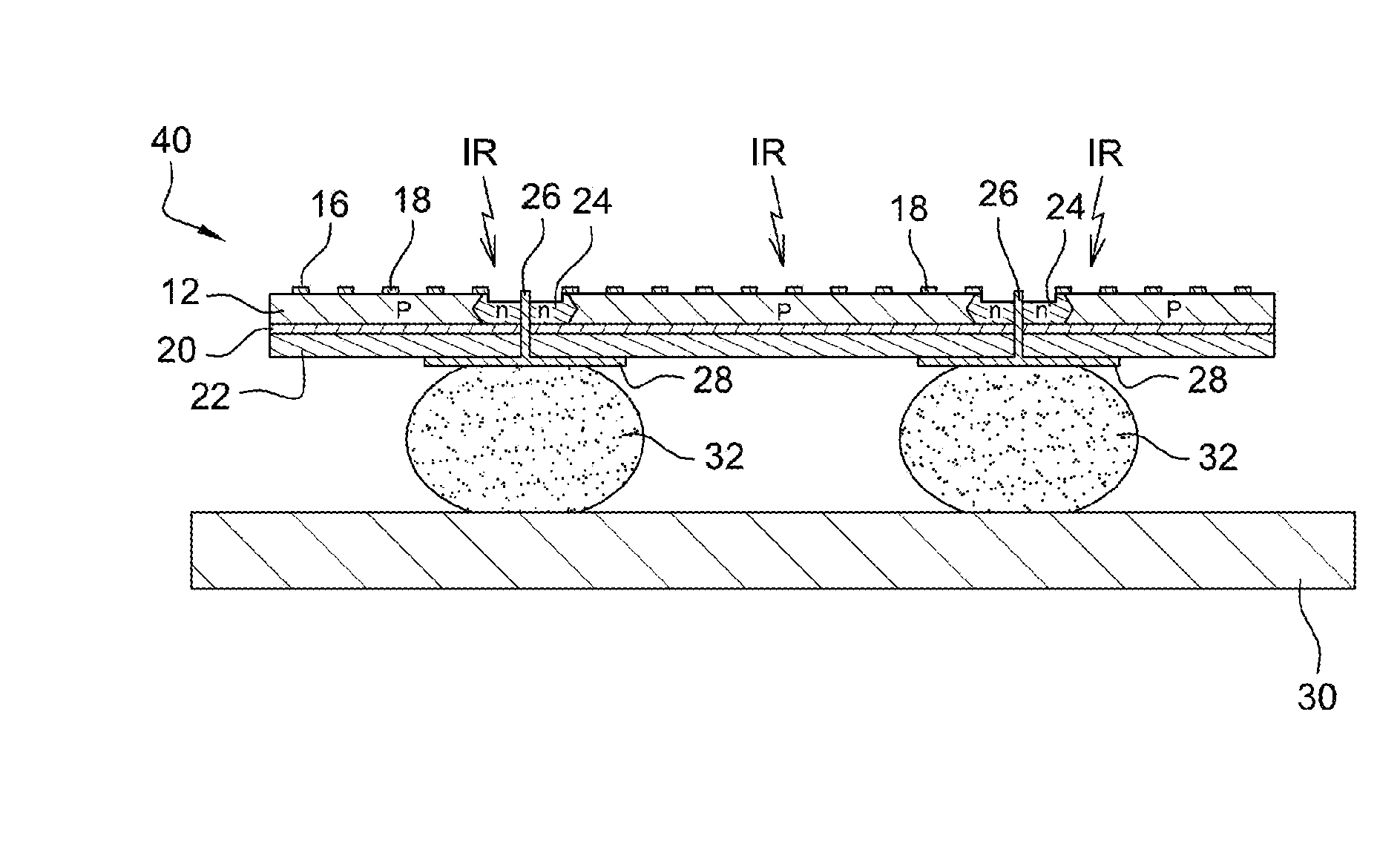
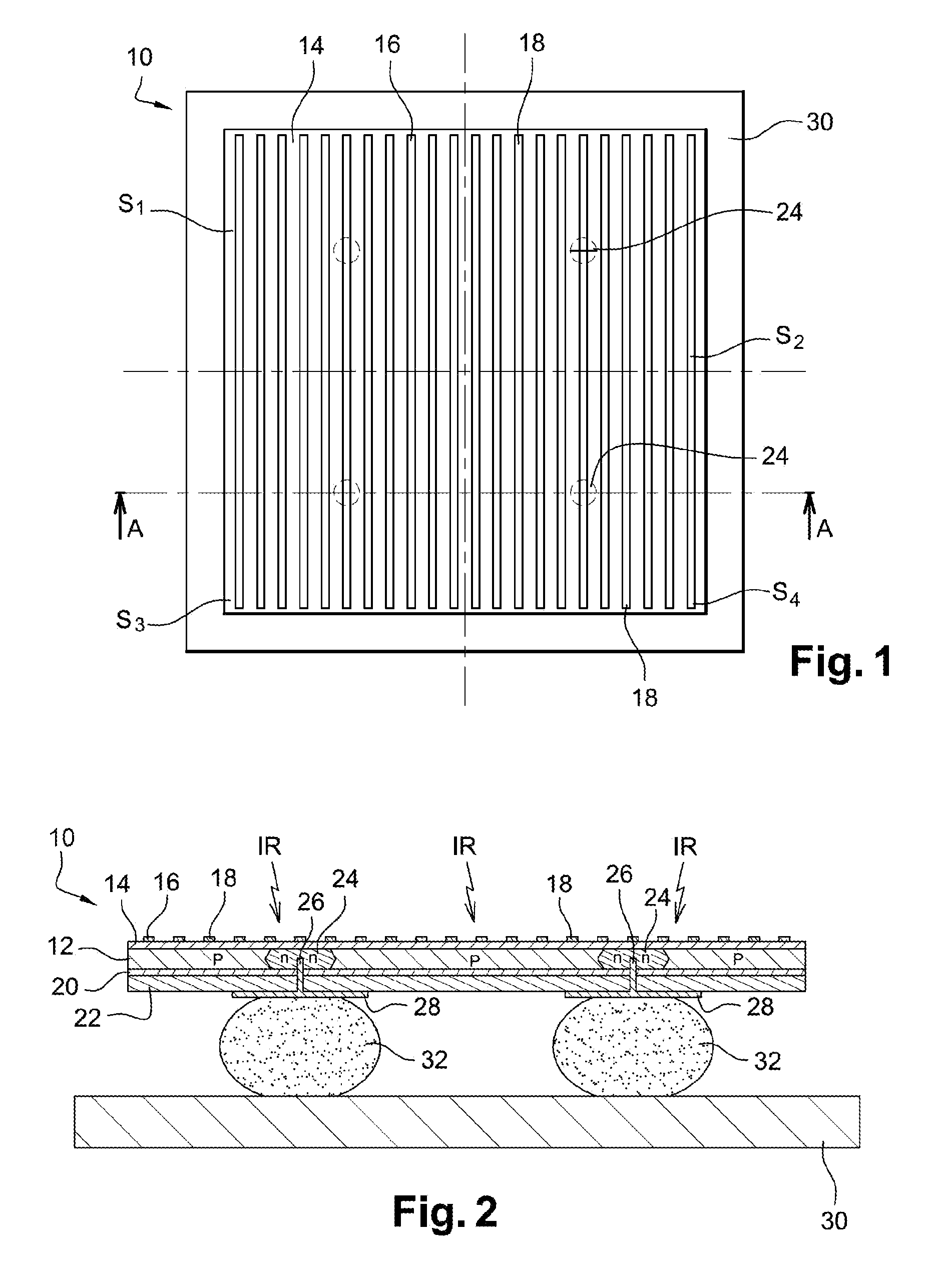
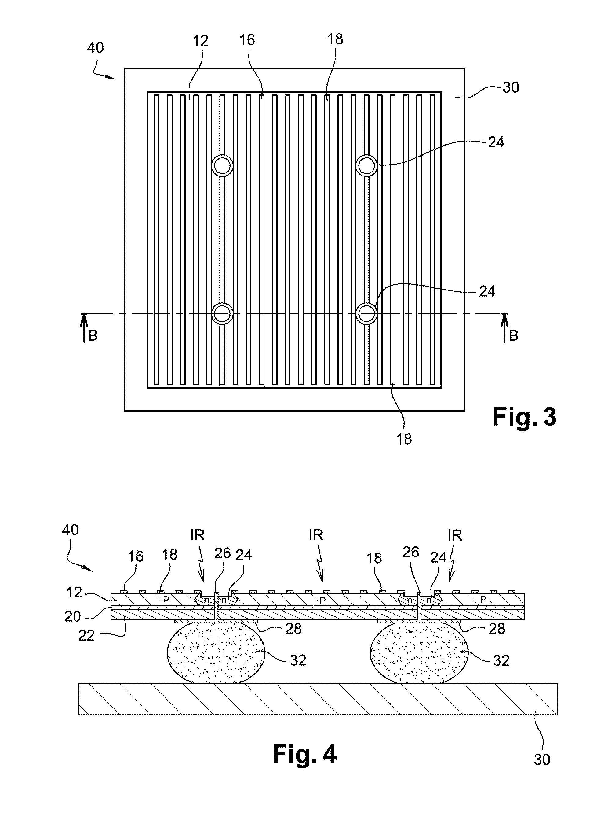
[0029]A two-dimensional photodetector according to the invention is shown in FIGS. 1 and 2 under the general reference 10. This example shows a photodetector that comprises 2×2 pixels.

[0030]Photodetector 10 comprises a semiconductor absorption layer 12 that is several hundred nanometers thick wherein incident photons create electron-hole pairs; it is, for example, a p-doped semiconductor layer made of CdHgTe or CdZnTe in order to detect middle infrared radiation (wavelength of 3 to 5 μm) and / or far infrared radiation (wavelength of 8 to 10 μm); an insulating passivation layer 14 that is several dozen nanometers thick and deposited on semiconductor layer 12; a metallic structure 16, made of gold for example, formed by identical, straight, parallel metallic strips 18 having a rectangular cross-section. Structure 16, together with semiconductor layer 12, forms a surface plasmon resonator, as is known in itself from the prior art; a dielectric tuning layer 20 that is several dozen nanom...


PUM


Abstract

This photodetector comprises a doped semiconductor layer; a reflective layer located underneath semiconductor layer; a metallic structure placed on semiconductor layer that forms, with semiconductor layer, a surface plasmon resonator, a plurality of semiconductor zones formed in semiconductor layer and oppositely doped to the doping of the semiconductor layer; and for each semiconductor zone, a conductor that passes through the photodetector from reflective layer to at least semiconductor zone and is electrically insulated from metallic structure, with semiconductor zone associated with corresponding conductor thus determining an elementary detection surface of the photodetector.

Description

CROSS REFERENCE TO RELATED APPLICATIONS[0001]This application claims priority under 35 U.S.C. §119 from French Patent Application No. 0959569 filed on Dec. 24, 2009 in the French Patent Office, the entire disclosure of which is incorporated herein by reference.FIELD OF THE INVENTION[0002]The present invention relates to the field of detecting electromagnetic radiation, especially infrared, using so-called metallic “plasmonic structures”.PRIOR ART[0003]One known method of detecting infrared radiation involves obtaining absorption of this radiation by a layer of small-gap semiconductor material such as CdHgTe for example. The absorption of photons by this layer then creates electron-hole pairs and the minority carriers thus produced diffuse or drift due to the effect of an electric field in the absorption layer so that they can subsequently be collected at the level of electrodes. Detection quality is then dictated primarily by the dimensions of the absorption layer.[0004]In fact, the...

Claims


Application Information

Patent Timeline
Patent Type & Authority Applications(United States)
IPC IPC(8): H01L31/052
CPCH01L31/1032H01L31/02002H01L27/1465H01L27/14625
Inventor GRAVRAND, OLIVIERDESTEFANIS, GERARDLE PERCHEC, JEROME
Owner COMMISSARIAT A LENERGIE ATOMIQUE ET AUX ENERGIES ALTERNATIVES
Why Eureka
Try Eureka