Semiconductor structure and formation method thereof

A semiconductor and top-level semiconductor technology, applied in semiconductor devices, semiconductor/solid-state device manufacturing, semiconductor/solid-state device components, etc., can solve the problems of semiconductor structure electrical performance to be improved, to improve self-heating effect, reduce temperature, The effect of increasing speed

Active Publication Date: 2017-08-11
SEMICON MFG INT (SHANGHAI) CORP +1
View PDF5 Cites 11 Cited by
  • Summary
  • Abstract
  • Description
  • Claims
  • Application Information

AI Technical Summary

Problems solved by technology

[0007] However, in the prior art, after the semiconductor device formed on the SOI substrate is bonded to other substrates (or wafers), the electrical performance of the formed semiconductor structure needs to be improved.

Method used


Image

  • Semiconductor structure and formation method thereof
  • Semiconductor structure and formation method thereof
  • Semiconductor structure and formation method thereof

Examples


Embodiment Construction

[0026] According to the background art, the electrical performance of the semiconductor structure formed in the prior art needs to be improved.

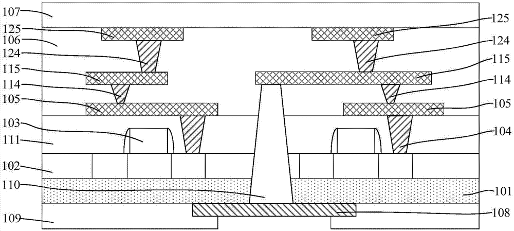
[0027] refer to figure 1 , figure 1 A cross-sectional schematic diagram of a semiconductor structure provided for an embodiment, including:

[0028] An insulating material layer 101; a top semiconductor layer 102 located on the surface of the insulating material layer 101, a gate structure 103 is formed on a part of the surface of the top semiconductor layer 102, and a side wall (not marked) is formed on the side wall surface of the gate structure 103, A doped region (not shown) is formed in the top semiconductor layer 102 on both sides of the gate structure 103, and the doped region is used as a source (Source) or a drain (Drain) of a transistor in the semiconductor structure; A first dielectric layer 111 covering the gate structure 103 and the doped region is also formed on the surface of the top semiconductor layer 102, and a fi...


PUM


Abstract

The invention provides a semiconductor structure and a formation method thereof. The semiconductor structure comprises a first opening which penetrates through a first dielectric layer and isolating structures which are arranged between adjacent transistor regions and an insulating material layer; a first thermal conducting layer which fully fills in the first opening, wherein the thermal conductivity of the first thermal conducting layer material is greater than that of the isolating structure material; zeroth conductive plugs which are arranged on the surface of a doped region and penetrate through the first dielectric layer; a zeroth conductive layer which is arranged on the first dielectric layer and electrically connected with the zeroth conductive plugs; a second dielectric layer which is arranged on the first dielectric layer and covers the zeroth conductive layer, wherein an interconnection structure electrically connected with the zeroth conductive layer is formed in the second dielectric layer; carrier wafers which are bonded with the surface of the second dielectric layer and the surface of a top conductive layer; a through hole which penetrates through the insulating material layer and is electrically connected with the interconnection structure; and an underlying conductive plug which fully fills in the through hole. The problem of the self-heating effect of the semiconductor structure can be improved and the electrical performance of the semiconductor structure can be improved.

Description

technical field [0001] The invention relates to the technical field of semiconductor manufacturing, in particular to a semiconductor structure and a forming method thereof. Background technique [0002] With the advancement of semiconductor technology, integrated circuits are developing towards high integration, high speed and low power consumption. The process of bulk silicon (Bulk Silicon) substrates and bulk silicon devices (devices manufactured based on bulk silicon substrates) is approaching Physical limits, severe challenges are encountered in further reducing the feature size of integrated circuits. At present, the industry believes that silicon-on-insulator (SOI: Silicon on Insulator) substrates and SOI devices are one of the best solutions to replace bulk silicon and bulk silicon devices. [0003] SOI substrate is a kind of substrate used in the manufacture of integrated circuits. Compared with bulk silicon substrates currently widely used, SOI substrates have many...

Claims


Application Information

Patent Timeline
Patent Type & Authority Applications(China)
IPC IPC(8): H01L23/373H01L23/367H01L23/48H01L21/768
CPCH01L21/76898H01L23/367H01L23/373H01L23/3738H01L23/481H01L21/76264H01L23/3677H01L21/4882H01L21/76802H01L21/76877H01L21/84H01L23/3672H01L23/5226H01L27/1203
Inventor 葛洪涛包小燕
Owner SEMICON MFG INT (SHANGHAI) CORP
Why Eureka
Try Eureka